EEZ DIB DCP405 Power module
|
Current version |
r3B3 |
|
Status |
Completed, ready for production |
|
PCB manufactured |
Yes (r3B3) |
|
PCB assembled |
Yes (r3B3) |
|
BOM |
Yes (TME, Mouser, Digikey, Farnell, RS) |
|
File repository |
https://github.com/eez-open/modular-psu/tree/master/dcp405 |
|
License |
|
|
Contributions |
|
Output power terminals |
Series |
Parallel |
Split rails |
Common ground |
|
Yes |
Yes |
Yes |
Yes |
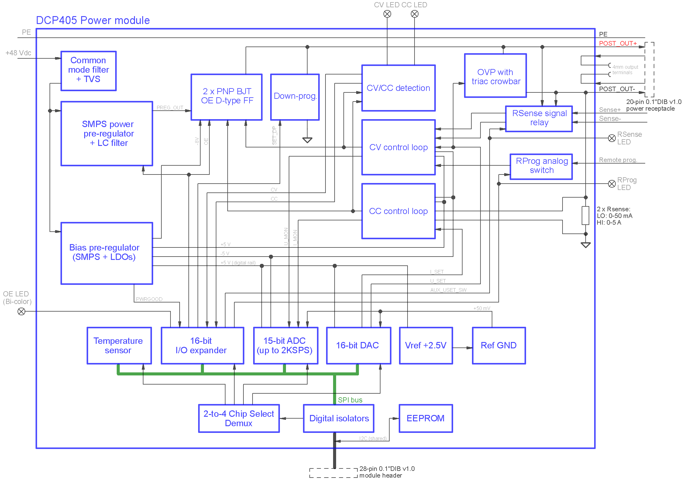
The DCP405 power module is programmable DC source that can deliver up to 40 V and 5 A using the hybrid topology of switching pre-regulator and linear (series) post-regulator. It is upgraded version of the Power board used in the H24005 project. Couple with another module it is possible to provide up to 80 V (in series) or up to 10 A (in parallel). The coupling is accomplished under firmware control thanks to power relays located on the BP3C backplane. Table above shows module’s all coupling possibilities. When uncoupled its output is isolated (“floating”).
Feature list
- Power input: 48 Vdc (e.g. Mean Well LRS-150F-48)
- Max. output power: 200 W (limited to 155 W due to Mean Well AC/DC module)
- Voltage regulation (CV), 0 – 40 V. Voltage set resolution (U_SET): 16-bit, read resolution (U_MON): 15-bit
- Current regulation (CC) with 2-range (50 mA, 5 A) software auto-ranging function. Current set resolution (I_SET): 16-bit, Current read resolution (I_MON): 15-bit for each range
- On-board power pre-regulator and bias power supply
- On-board OVP with triac crowbar and two fuses
- Down-programmer
- Output enable (OE) circuit with LED indicator combined with coupling indication
- On-board Ø4 mm safety sockets (19 mm/0.75” pitch)
- 20-pin pass-thru connector for output terminals coupling with other Power boards
- Remote voltage sense with LED indicator and inverse polarity protection
- Remote voltage programming with LED indicator
- Galvanically isolated SPI bus for communication with the MCU board
- I2C EEPROM for storing board specific configuration and calibration parameters
- I2C Temperature sensor
- Dimensions: 185 x 95 mm, 2-layer PCB
Power pre-regulator
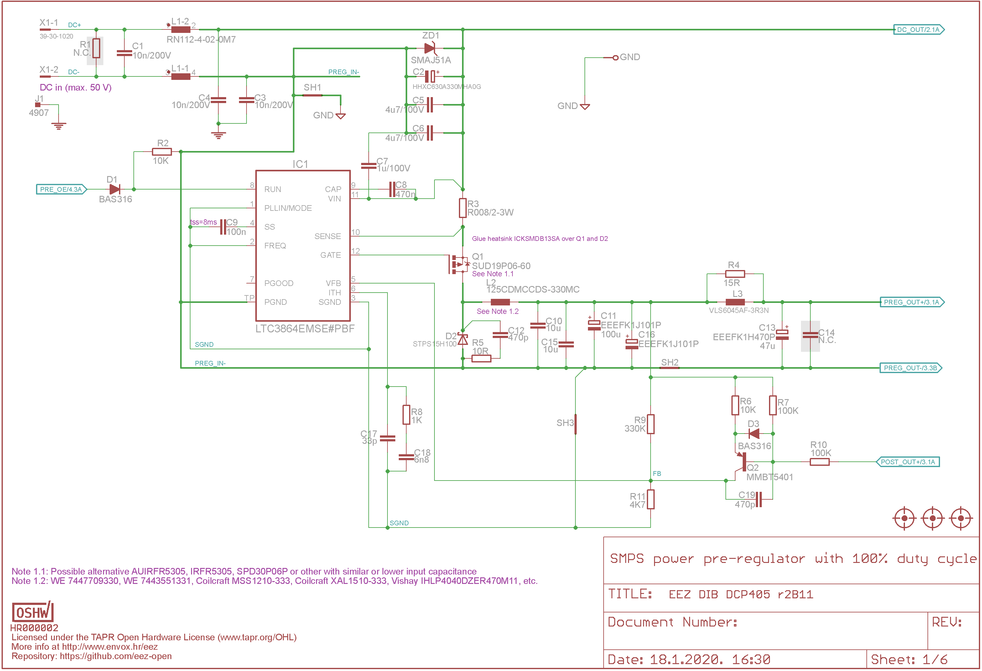
The power pre-regulator section in essence is the same as one used in H24005 Power board, but with few details omitted such as synchronization of switching frequency with an external source, reduced ripple mode of operation when pre-regulator is bypassed, and optional AC power input, i.e. only +48 Vdc power input is accepted on 2-pin power connector (X1). The PE (protective earth) connection is provided separately (J1) and ZD1 guards against over-voltage and reverse voltage faults.
Bias power supply
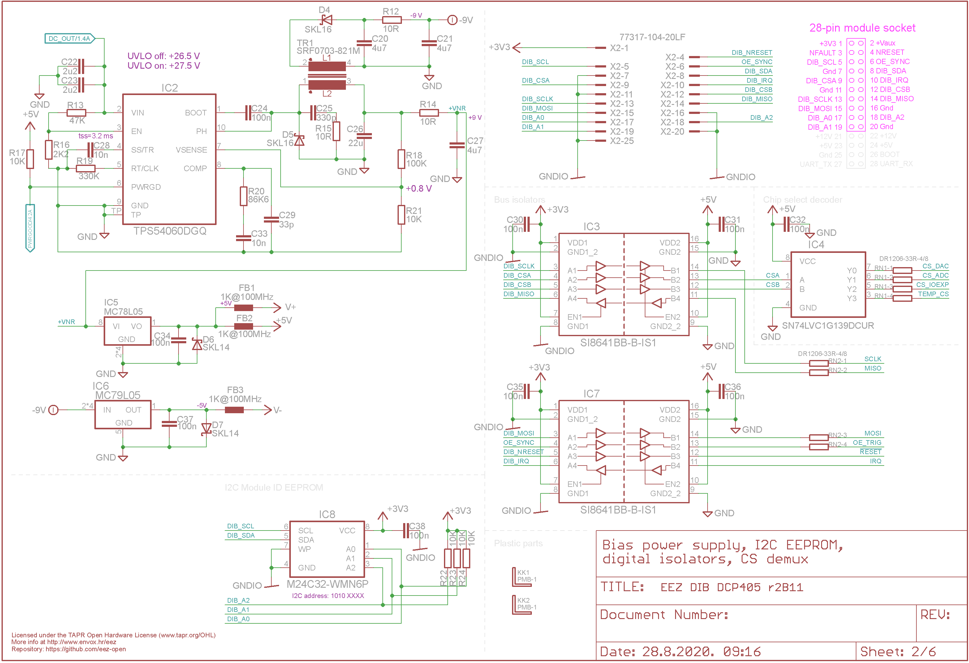
The bias power supply is built around low power buck step-down converter (IC2), and thanks to coupled inductor (TR1) it provides both positive and negative rails that are further regulated with simple linear regulators (IC5, IC6) to power all analog and digital logic with +/-5 V. For better separation between analog and digital power, +5 V is split with two ferrite beads (FB1, FB2) right on the IC5 output.
The IC2 also provides POWERGOOD signal that indicates MCU what is module’s power condition. It is related to UVLO (under-voltage lockout) functionality that is controlled with voltage divider consists of R13, R16. Therefore the step-down converter will cut-off power when input voltage drops below +26.5 V, and starts again when it rises above +27.5 V.
EEZ DIB interface
The DCP405 module interface with the MCU module is accomplished over the 28-pin (only 20-pin are used) 0.1” right angled header (X2). Since its power output has to be isolated (“floated”) all digital control lines has to be isolated. Therefore two high speed digital isolators (IC3, IC7) are used. Additionally, 2-to-4-line decoder (IC4) is also deployed because EEZ DIB v1.0 specification offers only two SPI CS (Chip Select) lines while DCP405 comes with four SPI devices.
Onboard I2C EEPROM (IC8) provides storage for module-specific information such as its ID, calibration data, working hours counters, etc. Please note that it is on the A-side of the isolation barrier, because the same I2C bus is shared among all modules (that includes AUX PS module, too).
Power post-regulator
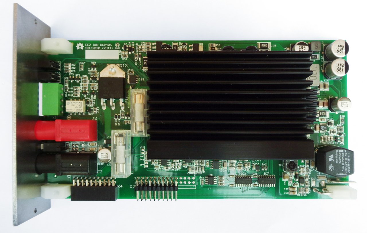
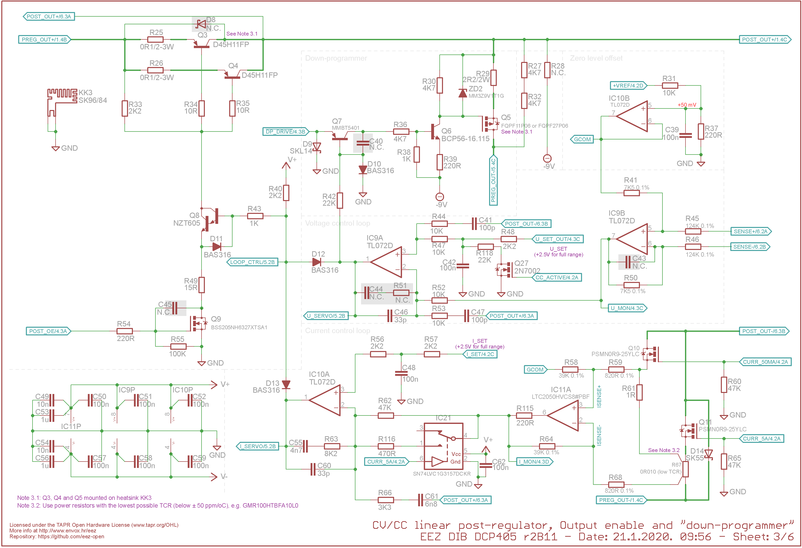
The post-regulator regulation (“pass”) element is PNP BJT, actually two of them (Q3, Q4) connected in parallel with current balancing power resistors (R25, R26). Their thermal coupling is also good since they are sharing the same heatsink and are mounted close to each other as shown on Fig. 5. The output voltage is controlled by two control loops: constant voltage (by IC9A, IC9B), and constant current (by using IC10A and IC11). In general, only one can be active at a time. Diodes D12 and D13 ensure that the output signal from one of the control loops does not affect the other loop.
The precision +2.5 V voltage reference (IC14, Fig. 7) is used for both control loops in supervising output voltage and current. Therefore, the gain in both control loops must be adjusted so the output range returns a positive value between zero and +2.5 V. That is done by selecting the feedback loop resistors for IC9B and IC11 which are connected as differential amplifiers. For example, if we’d like to have the output voltage in the range from zero to 40 V, IC9B’s gain must be 2.5 / 40 = 0.0625 (in effect, the output signal measurement must be attenuated by a factor of 16).
In practice, due to component tolerances, it is likely the highest values (e.g. 40 V) will not be reached, and a few tens of mV below maximum voltage will be the actual limit when the maximum DAC voltage is applied to the non-inverting input of IC9A.
The same problem can be expected on the other end of the voltage range; the minimum DAC voltage will not get the output voltage down to zero, but to only a few tens of mV above zero. This issue is more important, because it requires a negative DAC voltage – not possible with the DAC chip used (IC16, Fig. 7) without adding an additional operational amplifier. Fortunately such “shrinking of range” can be easily overridden with two simple changes:
- at the high end, we need to change the gain factor, and
- at the low end, move the reference ground potential from zero to, say, +50 mV (applied on IC9B and IC11 non-inverting inputs)
The voltage loop gain (for IC9B) is set to ~0.061 with a combination of 7.5 kΩ (for R41, R50) and 124 kΩ (for R45, R46). For the current loop (IC11), the gain is reduced from an “ideal” of 50 (i.e., 5 A across a 10 mΩ sense resistor gives 50 mV and 2.5 V / 0.05 V = 50) to 47.56 by using combination of 39 kΩ (R58, R64) and 820 Ω (R59, R68).
A new reference ground potential of about +50 mV is derived from a +2.5 V reference (IC14) by using the voltage divider R31, R37, and buffering it via IC10B. The offset on the lower programmed output value must be taken into account in firmware, however.
Current sensing and ranges
The output current is measured by the voltage drop across a current sense resistor (R61 or R67) for two ranges: LOW (up to 50 mA) and HIGH (up to 5 A). It is important to take into account any heating of the high range current sense resistor, since it decreases accuracy because its resistance is temperature dependent. Choosing a resistor with a low TCR even while keeping dissipation low will be best. Using the 10 mΩ the dissipated power will be 250 mW. The resistor chosen for R67 has a TCR of 20 ppm/oC (declared for 20 to 60 oC).
Selecting the current range is done by switching between two current sense resistors using MOSFETs Q10 and Q11 with low Rds(on) that is important when high range is selected to reduce the heating which might affect measurement precision regardless of the current sense resistor temperature stability (TCR).
Digital control
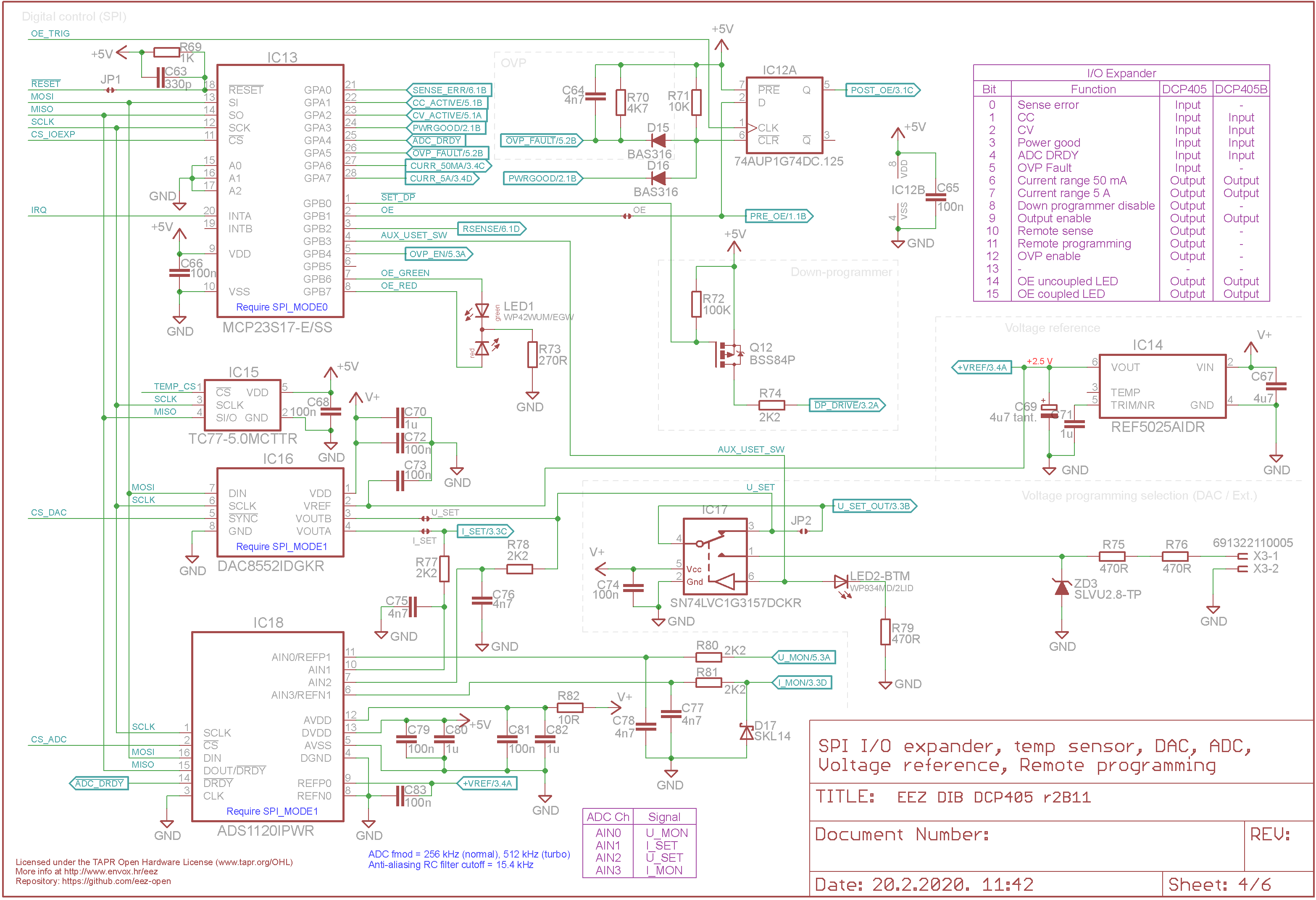
The post-regulator is an analog circuit controlled by analog control loops. Any control function done digitally (e.g., via MCU firmware) requires signal conversion. Four SPI devices are added to support this requirement (Fig. 7):
- Dual channel 16-bit Digital to Analog Converter,
- Four channel (multiplexed) 15-bit delta-sigma (ΔΣ) Analog to Digital Converter,
- 16-bit I/O expander
- Temperature sensor
Down-programmer
The down-programmer can be thought of as an internal load across the power supply’s output terminals that helps bring the output voltage down quickly. The primary function of the down-programmer is to discharge the output capacitor (C91+C92) but in some cases this feature may be used as a load to the connected device.
It’s sinking capability can be calculated using the following equation:
|
|
Isink, max = (VZD2 – Vth[Q5]) / R29. |
|
Therefore for the current setup, and if we use as average Q5’s Vth of 3 V it is (9.1 - 3) / 2.2 = 2.78 A. This is a huge current, but it last in milliseconds. Nevertheless that has to be taken into account when repetitive output voltage programming sequence is required with short step duration (i.e. in tens of milliseconds) with step difference of 5 V or more to avoid overheating of Q5 that has to dissipate voltage difference between programmed steps. That is especially important if huge capacitive load (e.g 470 μF and more) is connected to the module power output.
Digital to analog converter (DAC)
The DAC (IC16) is used to control the voltage and current for the power supply. Using a SPI bus, the MCU communicates with the DAC to program a new voltage at the DAC’s outputs (U_SET and I_SET). This chip also includes a power-on reset circuit which ensures that the DAC outputs power up at zero, and remains there until an explicit command from the MCU firmware takes place.
The range of voltage the DAC can manage is determined by the voltage at its reference pin (Vref) which is connected to the precision voltage reference of +2.5 V (IC14).
Analog to digital converter (ADC)
The ADC (IC18) is equipped with a four channel input multiplexer, and can manage up to 2 000 samples per second. It’s used to measure voltage and current control loops levels (U_MON, I_MON), but also the DAC outputs (U_SET, I_SET). The ADC used is a 16-bit bipolar device which gives 15-bit resolution (positive half) of the full scale (the negative half is partially used; it monitors to some extent down-programmer sinking).
16-bit I/O expander
An SPI I/O expander (IC13) is used to collect various digital signal inputs and to enable/disable various functions as shown in table below.
|
# |
Direction |
I/O name |
Active |
Description |
|
0 |
Input |
SENSE_ERR |
Low |
Reverse remote sense polarity detected |
|
1 |
Input |
CC_ACTIVE |
Low |
CC (constant current) mode of operation is active |
|
2 |
Input |
CV_ACTIVE |
High |
CV (constant voltage) mode of operation is active |
|
3 |
Input |
PWRGOOD |
High |
Power good has been received (i.e. bias power is operational) |
|
4 |
Input |
ADC_DRDY |
Low |
New A/D conversion data are ready |
|
5 |
Input |
OVP_FAULT |
High |
HW OVP circuit is tripped |
|
6 |
Output |
CURR_50MA |
High |
Set the low current range resistor |
|
7 |
Output |
CURR_5A |
High |
Set the high current range resistor |
|
8 |
Output |
SET_DP |
High |
Enable (or disable) the down-programmer circuit |
|
9 |
Output |
OE |
High |
Enable or disable power output |
|
10 |
Output |
RSENSE |
High |
Voltage remote sensing selection (internal / remote) |
|
11 |
Output |
AUX_USET_SW |
High |
Voltage programming source selection (DAC / external) |
|
12 |
Output |
OVP_EN |
High |
Enable HW OVP circuit |
|
13 |
– |
– |
– |
Not used |
|
14 |
Output |
OE_GREEN |
High |
Power output enabled (uncoupled) |
|
15 |
Output |
OE_RED |
High |
Power output enabled (coupled) |
Temperature sensor
On-board temperature measurement is used for determining fan speed and for software based OTP (over-temperature protection) and it is achieved using the dedicated SPI temperature sensor (IC15) that is positioned close to heatsink, and for better temperature transfer, its ground pin is coupled with the heatsink. It provides temperature with ±2 °C (max.) accuracy from -40 °C to +85 °C.
Remote programming
It is already stated that output voltage is regulated with CV control loop that is consists of IC9A and IC9B that is programmed using the DAC’s U_SET output. Additionally, the DCP405 offers voltage programming by supplying a positive analog signal (+2.5 V for the full scale) on the push-in terminal input X3-1 (and X3-2 as return). Only one reference signal can be used at a time which is managed with an analog multiplexer/switch (IC17). The default setting is internal (i.e. DAC output). Analog programming is faster, but additional care must be taken to stay within the safe working range even though there is protective TVS diode ZD3.
Mode of operation detection and indications
When its output is enabled, the DCP405 can work in one of the following operational modes:
- CV (constant voltage): the voltage control loop circuit (IC9) is setting the output voltage, and CV LED is active
- CC (constant current): the current control loop (IC10A, IC11) is setting output voltages, and thereby limiting output current, and CC LED is active,
- UR (unregulated, i.e. not regulated): neither the output voltage nor output current are controlling the DCP405’s output, and both LEDs are active. In normal operation this mode is entered for a very short time while regulation is changed from CV to CC mode or vice versa. However, if DCP405 stuck in this mode that is indication that regulation is not possible, i.e. the output cannot be set to programmed voltage or current.
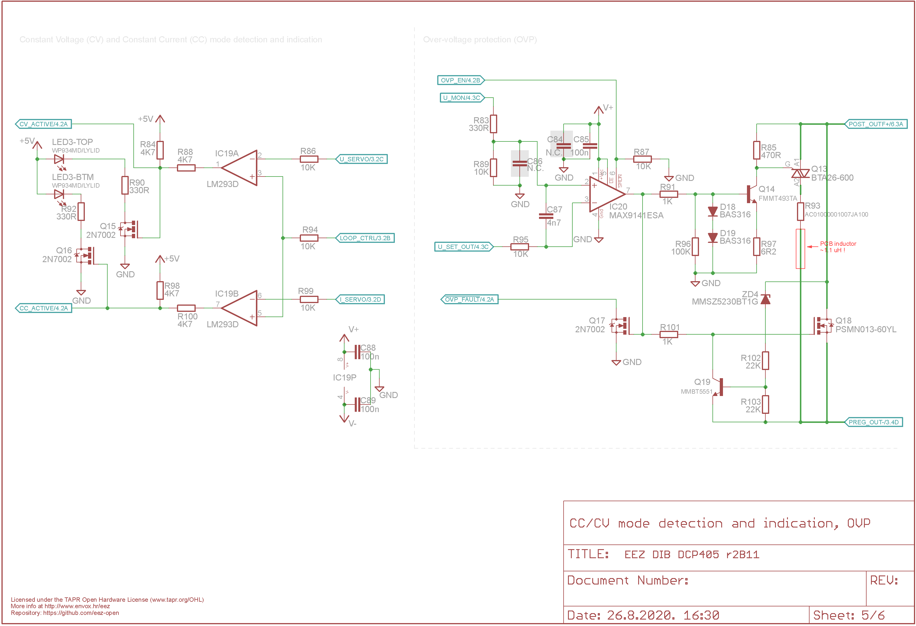
The CC and CV circuits use comparators (IC19A, IC19B) that compare control loop outputs (U_SERVO, I_SERVO) against LOOP_CTRL signal, or simply the voltage difference on diodes D12, D13 that separates CV and CC control outputs. The signals produced are level shifted for TTL inputs (using the R84, R88 and R98, R100 voltage dividers).
OVP crowbar
The OVP (over-voltage protection) circuit is added to act as a very fast protection in situations when output voltage erroneously rise above set value. It purpose is to protect DCP405 when e.g. battery or other power source is connected to the output terminals with voltage higher the programmed. It also protects connected load in case that something badly wrong is happened with the post-regulator that it voltage uncontrollably rises. The OVP circuit is consists of two main parts: fast comparator (IC20) and “crowbar” circuit where triac Q13 acts as crowbar driven by Q14. Voltage divider R83, R89 connected to the output voltage sets comparator threshold that is set to about 5 % above set voltage.
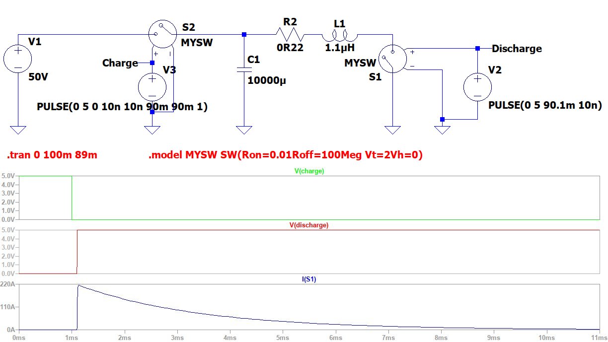
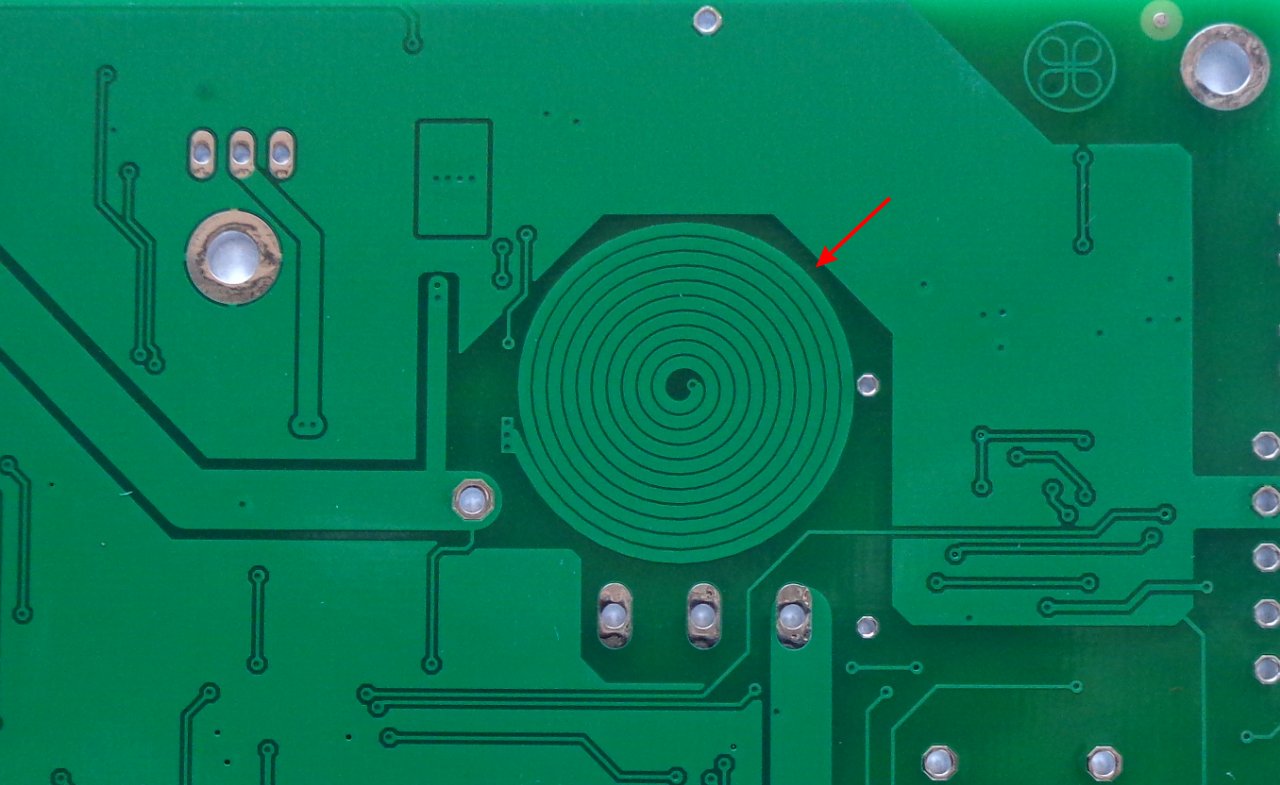
Note that in series with triac a high current resistor (R93) and PCB inductor (Fig. 10) are added to smooth possible current rising edge which can be in case of large capacitor discharge very high. For example, a capacitor of 10 000 μF charged to 50 V can provide up to 220 A when it is attenuated with 0.22 Ω and 1.1 μH as shown simulation on Fig. 9. Such current peak is still below ITSM (Non repetitive surge peak on-state current) value of the selected triac, therefore the OVP should survive such type of event.
A triac based OVP can cover voltages of approximately +1.5 V and above. For this reason, a parallel MOSFET based OVP (Q18) was added. However it is not suitable for a higher voltage so its upper activity limit is set with Q19 biased with voltage divider that includes ZD4 (about +5 V).
Voltage sensing
Output voltage can be “sensed” locally or remotely. In the first case the sense inputs is connected to the power output (OUTF+, POST_OUT-). In the second case, the connection is done via the load’s input terminals using a separate cable connected directly to the load’s terminals. The firmware manages this through the signal relay (K1). The remote sensing cable can be shielded, but the cable shield must be connected to an PE terminal (X3-3) only on one end to avoid ground loop problems.
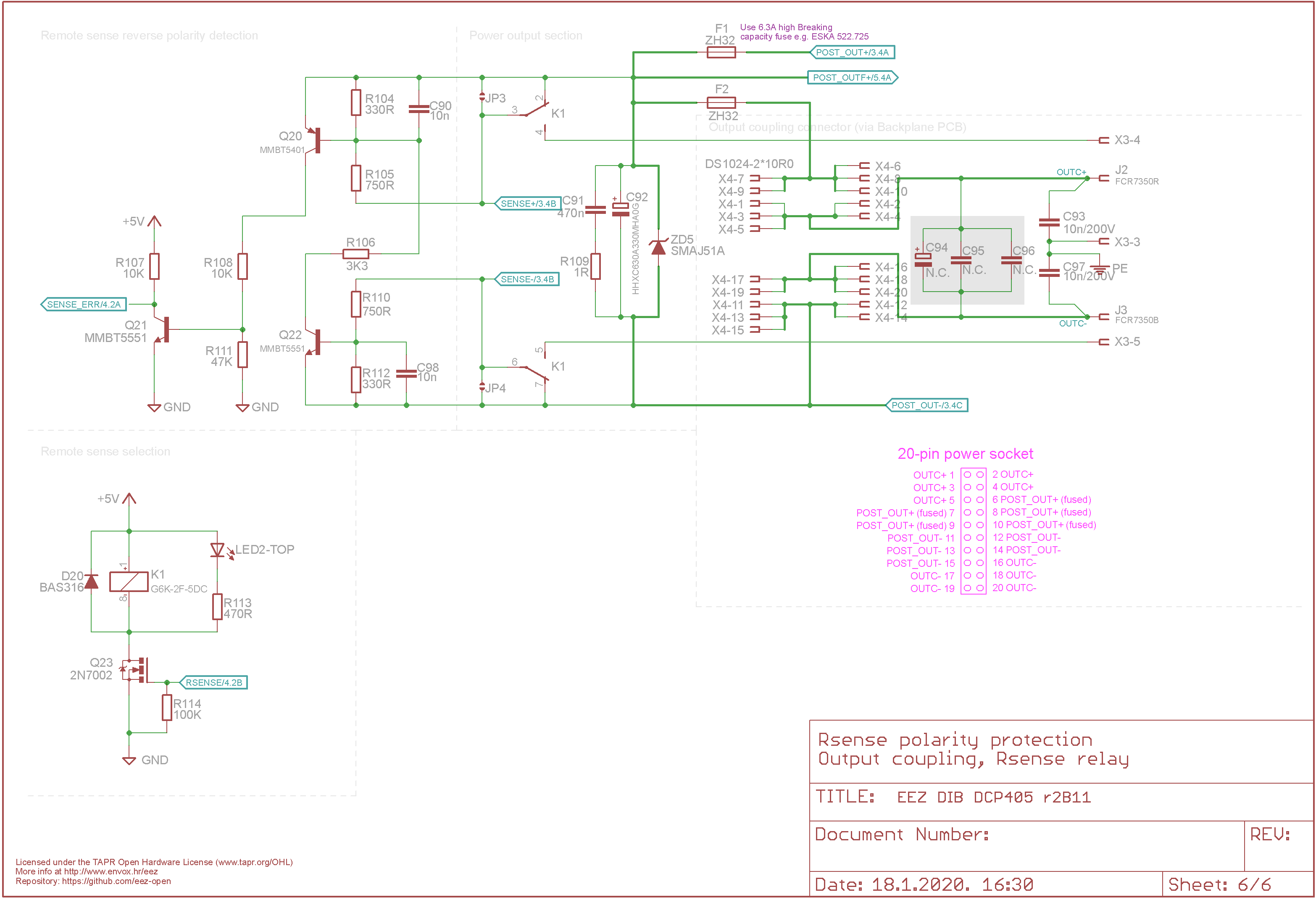
Remote voltage sensing is necessary to insure precise output voltage programming regardless of output current. It is essentially impossible to deliver power to a load with 1 mV precision without remotely sensing the voltage at the load’s input terminal, perhaps at the end of a cable just half a meter away from the output terminals. Output currents of a few amperes through insufficiently robust connection cables, or to load terminals with a resistance in miliohms, could easily produce a voltage drop across the cable from a few milivolts to even a few hundred milivolts. When using remote sensing, the output voltage actually supplied to the load is not measured at the power outputs but at the connected load terminals. The CV control loop (IC9B, Fig. 6) can compare that voltage against the programmed one, and all the voltage drops along the cable will have no effect. The technique is generally referred to as “Kelvin sensing”, or 4-wire measurement technique.
Remote sense reverse polarity detection and protection
Exposing the voltage sensing inputs to some external connection has disadvantages, however. The major one, not always obviously so, is that any or both of the sense cables can be mistakenly connected in a reverse polarity fashion that can ends up with unexpected results for the connected load. Internally, local sensing will be correct because the signal relay (K1) will insure the correct connection to the voltage control circuitry.
When remote inputs are disconnected from the load input power connectors, the DCP405 can still work safely because they will still be properly polarized thanks to R104, R105 and R110, R112. There will be only a small deviation in output voltage because of the addition of about 2 x 1 kΩ to the input voltage divider of IC9B.
However, if a sense wire is connected to the opposite polarity power output, there will be a serious fault condition for the input signal will have no relation to the channel attempting to ensure correct voltage and current to the load. There will be a maximum error bias within the CV control loop; it will try to compensate, and the end result will be the maximum possible voltage on the output (i.e. +40 V). This could easily result in irreparable damage to the connected load, especially if the set output current is high.
To avoid some of these unfortunate events, a reverse polarity detection circuit (Q20, Q22) has been added in parallel with the remote sensing inputs. It has two purposes: first, to immediately decrease output voltage, and to generate a SENSE_ERR signal (Q21) that will notify MCU to immediately disable output.
Reverse polarity power output protection
Mistakenly connected load such as battery to the power terminals could results with damage of one or more sections. Therefore the TVS (ZD5) is connected to the outputs. Replaceable fuse (F2) connected in series limits stress applied on diode.
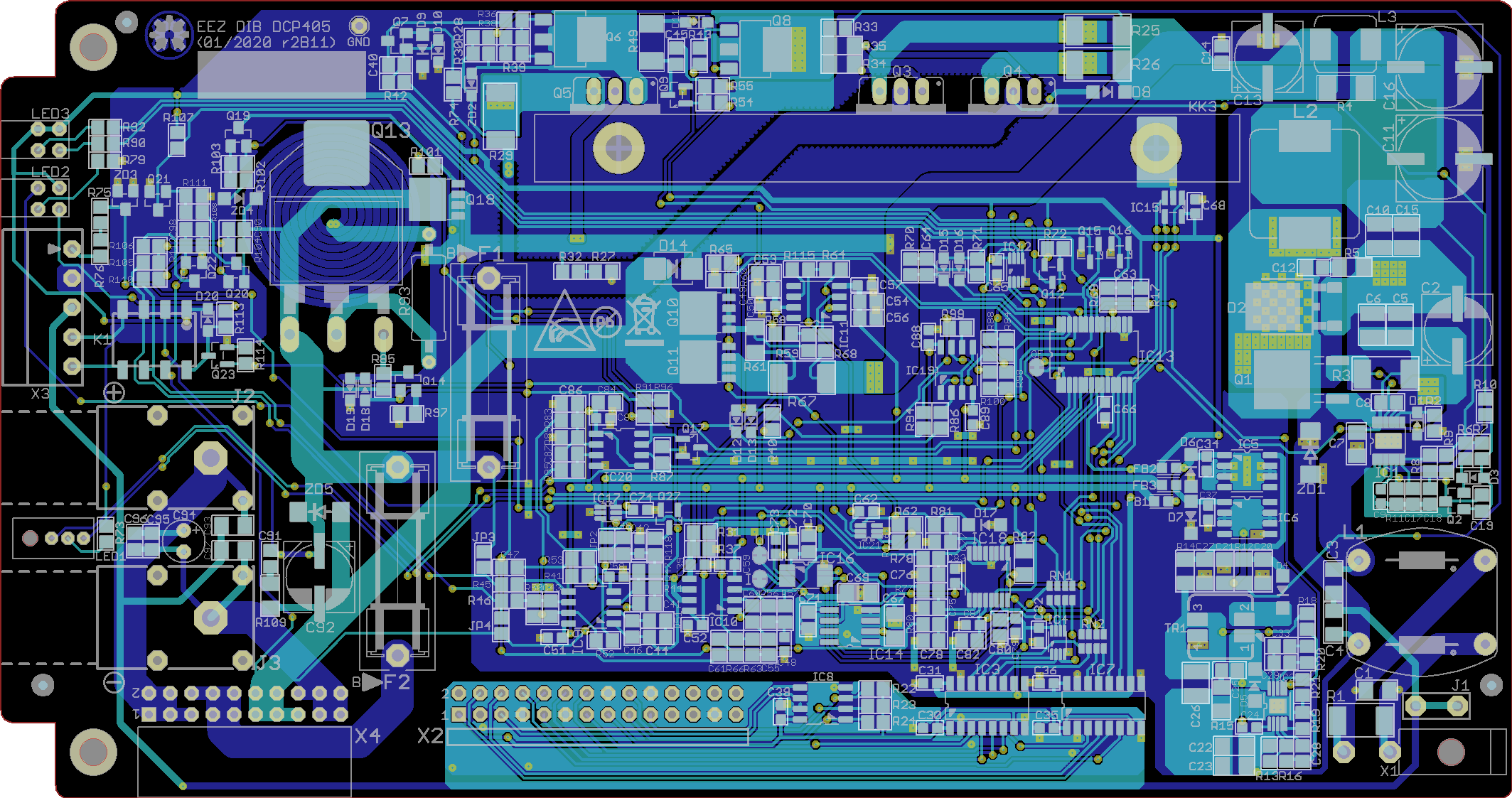
PCB layout

