EEZ PSU H24005 Building Instructions (r5B12)
A work in progress (Draft 0.6) – PDF version for download is available at the page end
Building instructions for prototype version r5B9 can be found here.
This project is rather different from the usual DIY sort. It will handle moderately high voltages (much higher than 5V or 3.3V logic levels or 12V systems), and very high currents (much more than just about any common electronic equipment in the consumer world except perhaps high power audio amplifiers). As a result, assembly mistakes are not likely to cause problems merely within the assembled project, but also to anything connected with it. Proceed carefully, make certain you have identified the correct part and location before installing anything. In fact, it will be worthwhile to read through these instructions before beginning. Restrain your eagerness a bit!
If you need assistance, please contact us using this form or post your problem on the EEVblog forum here. Or, feel free to open a New issue on GitHub here, but please check first to see whether a similar issue already exists).
The power supply (PSU) has four printed circuit boards (PCBs) on which parts may already be installed depending on how you ordered the assemblies. Most of these are surface mount devices (SMD) (tiny and with small or no ‘legs’). Only connectors, and few specialized parts (e.g. power resistors, PCB mounted AC/DC adapters, post-regulator power MOSFET, etc.) have legs that go through holes in the PCB, – they are through-hole parts (THT).
The SMD parts have been selected to be easily installable using (careful!) hand soldering, but will greatly benefit from the assistance of an illuminated magnifying glass, or a low magnification microscope. In general, a magnification of x8 to x10 should be more than appropriate. Almost all passive SMD components are 0805 size, but never smaller then 0603. Some of the IC packages are SOIC, TSOP, TSSOP; there are no bottom on any of the IC pin packages such as QFN or BGA as these are essentially limited to machine installation and reflow soldering.
Only two ICs (i.e., IC1, IC4 on the Power boards) have exposed tabs which cannot be readily installed using a soldering iron, and will probably need a hot air soldering station. Installing these requires different skills, examples of which can be found in many videos on the Internet with instructions on how to do so effectively by hand, without the use of solder paste stencils or reflow ovens.
1.1. Required tools
- A soldering iron with a conical tip example
- A hot air soldering station example (more than ordinary skill with a soldering iron may make this optional)
- Rosin core solder wire (0.25 mm diameter example, and 0.7 mm example). See below for more information.
- Some solder wick / desoldering braid example
- Some solder flux. This is often used, via an applicator (resembling a syringe) or a very small brush. As before this must be compatible with electronic parts, not the acidic types used in plumbing or stained glass work1. Example
- A magnifying glass with light (e.g., a desktop magnifier with a backlight) example or a microscope (also with a light) example
- A pair of self-locking tweezers (sometimes called a hemostat, from those used in medicine) example
- A pair of sharp non-locking tweezers example1, example2
- Isopropyl alcohol2
- A PCB holder example. SMD parts are small; do not sneeze or let the cat help. A dog’s friendly tail wag can be a disaster. A PCB holder really will help.
1.2. Test and measurement equipment
The basic tool needed for measurements is an oscilloscope. A high performance specification is not required (e.g., an elderly low frequency bandwidth scope would be fine if it works properly). But, if assembly is performed carefully (as it should be, and check everything more than once!) so that there are no mistakes (e.g., the wrong part value, or the right part installed in the wrong place, or inadvertent solder fragment shorts between parts or PCB traces, etc.) a multimeter (DMM) will be enough to check basic functionality. An adequate DMM need not be expensive, but beware that there is a large selection of inexpensive and effectively worthless DMMs on offer. Several of Dave Jones’ EEVBlog videos are DMM reviews, and at least two have been comparisons of several inexpensive meters.
During testing and taking measurements, please note that a channel’s negative output (OUT-) is NOT at ground potential with regard to the mains earth potential in the AC wiring. If you are using a multichannel oscilloscope which does not have isolated channels (the default!) you cannot simultaneously connect the test probe ground of one channel to a PGND point and another channel to an OUT- point. This will interfere with normal operation of the current control loop (IC6A, IC7) because the current sense resistor (R63 or R65) will be shorted out; as well, there is a real risk of damage to either test probes or oscilloscope circuitry, or both. Short of exotic and expensive oscilloscope probe accessories, limiting connections to one probe at a time is wise.
1.3. Where to start?
The total number of parts to be installed and soldered, or mechanically bolted, or both, is almost 800. At first glance, this might be discouraging, but it’s not really so bad. First, the two most demanding PCBs are the Power boards which are identical. You might assemble them side by side following the steps below, which might help catch an error in one of them. The AUX PS is the simplest, but it also has an AC mains section that requires great additional care. Wiring mistakes involving mains connections are dangerous, and potentially fatal. Check them at least twice, and then have someone else (ideally) check them again, before applying power. Finally, the physically largest part – the Arduino Shield – is only modestly populated, but also carries extra parts such as the touch-screen display, encoder, Arduino board, binding posts, etc and mechanically mates with the front panel. It must be assembled somewhat differently as a result.
The recommended starting point is to check that all parts from the consolidated BOM (bill of materials) are present, sorted by type and value, and are easily accessible. As you have probably already learned, simple SMD parts with 2-3 terminals (passives, diode, transistors) can be easily lost even if you have well arranged and clean benchtop. Therefore, instead of despairing, plan ahead and simply order a few more parts than needed, and be more careful next time. Small SMD parts can escape both self-locking and regular tweezers, and every attempt to find them after they have jumped away.
There are a few sensible methods of storing and sorting SMD parts: small part snapboxes (example), SMD storage books (example), etc. Each of them will be useful insofar as it can reduce the possibility of replacing one part mistakenly with another. That is especially important for SMD ceramic capacitors (e.g., MLCCs) which often do not have value labels.3
Selecting a single value at a time and placing it in the proper place on the PCB is of a paramount importance to ensure that PCBs are assembled correctly. Keeping all other parts safely to the side, off the work bench entirely, is not too much caution.
Once the required tools, the bare (or partially populated) PCB, and the needed parts are ready, it is necessary to find the proper installation positions and orientations, and in the case of unmarked parts, distinguishing it from otherwise identical parts. Part locations on the PCBs are all identified, but with respect to the schematic – IC3, R21, C42 and so on.
If you are using the Eagle PCB design program, then open the correct .brd file and, when populating the top layer make sure that among other layers 21, 25, and 27 are visible (see Top assembly selected layers.png). For assembling the bottom layer set layers 22, 26, and 28 as visible (see Bottom assembly selected layers.png).
The freeware edition of Eagle also allows you to switch .brd files and layers on and off; this can be very useful.
When installing Eagle is not an option, you can use the following images:
- AUX PS r5B12a assembly (top layer).png
- AUX PS r5B12a assembly (bottom layer).png
- Arduino shield r5B12 assembly (top layer).png
- Arduino shield r5B12 assembly (bottom layer).png
- Power board r5B12 assembly (top layer).png
- Power board r5B12 assembly (bottom layer).png
This sequence of PCBs is not mandatory during assembly, but is a logical sequence since the AUX PS board is required for powering the Arduino shield and the Arduino shield is required for controlling the Power boards. This sequence is also sorted by PCB complexity starting with the simplest. If not otherwise specified, we recommend that parts be soldered in the following order on the same layer:
- SMD IC that require hot air soldering (i.e. IC1, IC4)
- Small SMD parts (e.g. passives (i.e., resistors and capacitors), diodes, transistors, etc.)
- SMD ICs
- Bulk SMD parts electrolytic capacitors, power inductors, MOSFETs and diodes) and
- THT parts (connectors, switches, chokes (i.e., inductors, etc.)
1.4. Default jumper positions
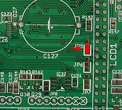
For various reasons, in a few places on the PCBs, a jumper section is used where a zero-ohm resistor (these look like a real resistor, though almost always with a single mid spaced black band, but can also be a plain wire) o define the signal path. Some of them define behavior of the circuits (e.g. JP5, JP6, and JP7) and when wired in the wrong way, or left unpopulated, can cause difficulties. In particular, the firmware running the PSU might not be able to control it properly. To simplify the assembly process, a clear silk screen mark has been added next to zero-ohm resistor default positions that should insure proper functionality with the current firmware revision. In the image below, the jumpers noted are marked, and red rectangle indicate the place for a zero-ohm resistor with “U” shaped silk screen mark.
1.5. AUX PS r5B12a assembly
NOTE: Some of the wiring on this PCB is connected to the mains AC. This requires that all parts and connectors be installed with NO errors. Failure to do so may damage parts, the power supply itself, or you. Check everything very carefully. Furthermore, if you are providing the parts (and even if you ordered them as part of a kit), do check to make certain they are the correct part, with the correct ratings in all respects. It may be a reassurance that part color is not important.
The schematic for this board is on sheets 6/12 and 7/12. We recommend the following steps:
- Fan control,
- AC input terminal and protection,
- Soft start/stand-by (Q20, Q21, OK1, OK2),
- Power relay (K_DOU2),
- Dual output AC/DC module (TR1) and
- THT connectors (X5, X6, X7, X8, X10, X11)
Testing of the fan control must be postponed until the Arduino Shield is available. Also, it will require preparation of the fan cable which comes without a connector (fans differ considerably).
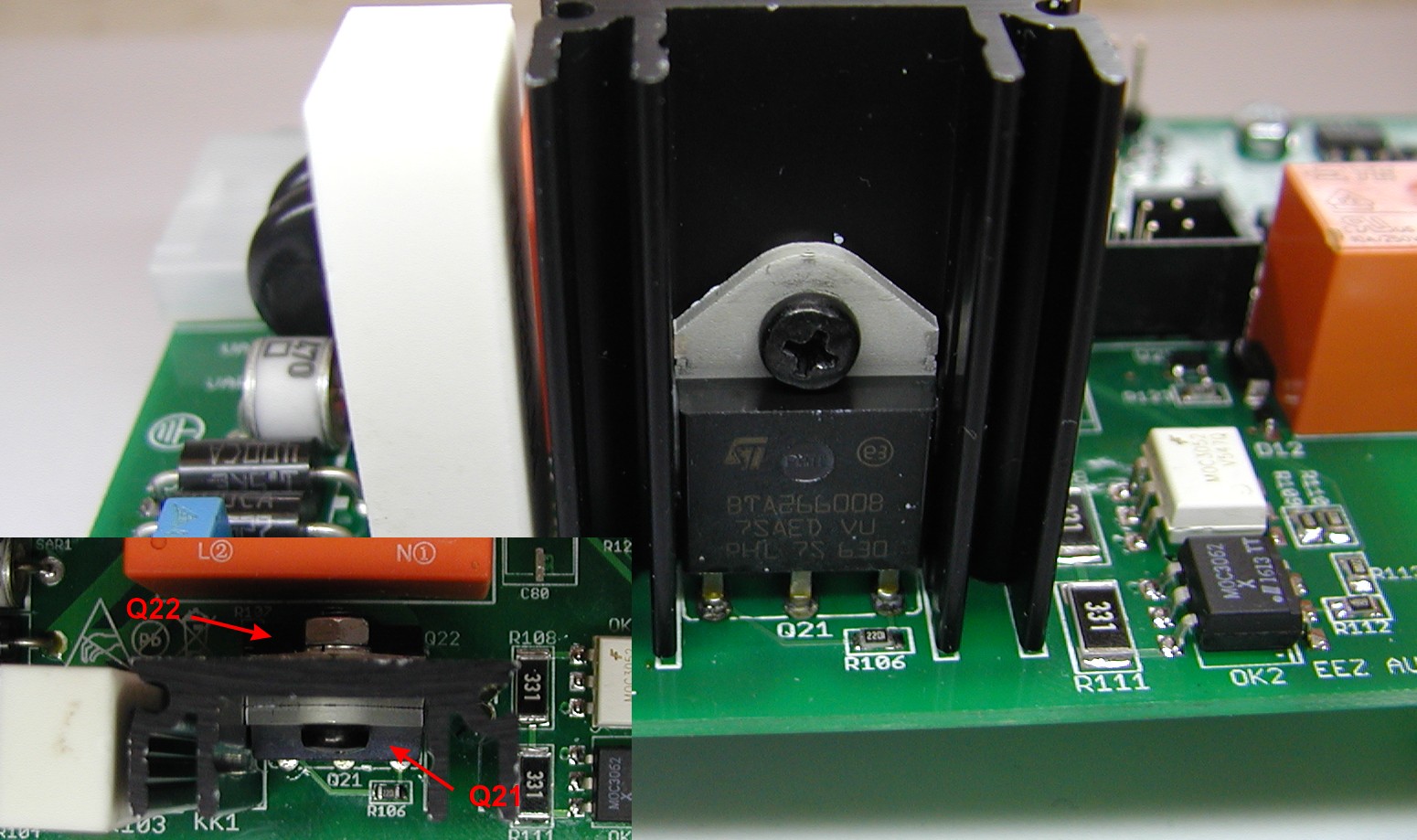
The AC input terminal and protection section contains only THT parts that MUST be carefully and correctly soldered. Soft start/stand-by triacs Q21 and Q22 share the same heatsink (KK1) though mounted on opposite sides, using a single screw and nut (Fig. 2). They should be mechanically mounted before soldering. Another possibility is to solder the heatsink first and then mount a triac on each side and then solder their terminals; this is somewhat tricky, however. Take care that power resistor R103 is of proper type (i.e., wirewound), properly rated voltage, and proper power rating.
The X5 connector must be mounted after the surrounding SMD parts (R122, OK3, ZD6, Q25), otherwise it will be difficult to mount them without damaging X5 by touching it unintentionally with the soldering iron’s body or its tip.
Finally, place TR1 as the last part on the top PCB layer. Now it’s possible to test the +5 V power supply by carefully applying AC mains on the X4 pin 1, 2 and 5.
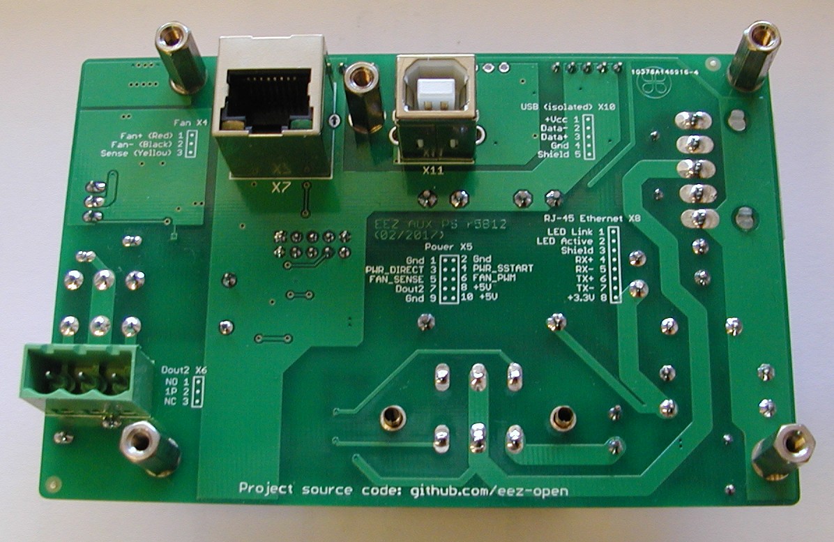
On the bottom layer, only three parts must be mounted – DOUT2 (X6), Ethernet (X7) and USB (X11) connectors. If you got the customized enclosure with pre-drilled holes on the rear panel, you can mount the PCB on the rear panel first (using 14 mm spacers), and then solder the bottom of the board connectors. This insures everything fits mechanically.
1.6. Arduino Shield r5B12 assembly
We don’t have a suggested assembly order for this assembly. One possibility is to simply follow the order of sheets in the consolidated schematics related to this board (i.e., sheets 8/12, 9/12, 10/12, 11/12, and optionally 12/12) and to leave the following parts until the end:
- Power relays (K_SER, K_PAR) – due to their size
- Super capacitor (C112) for RTC backup
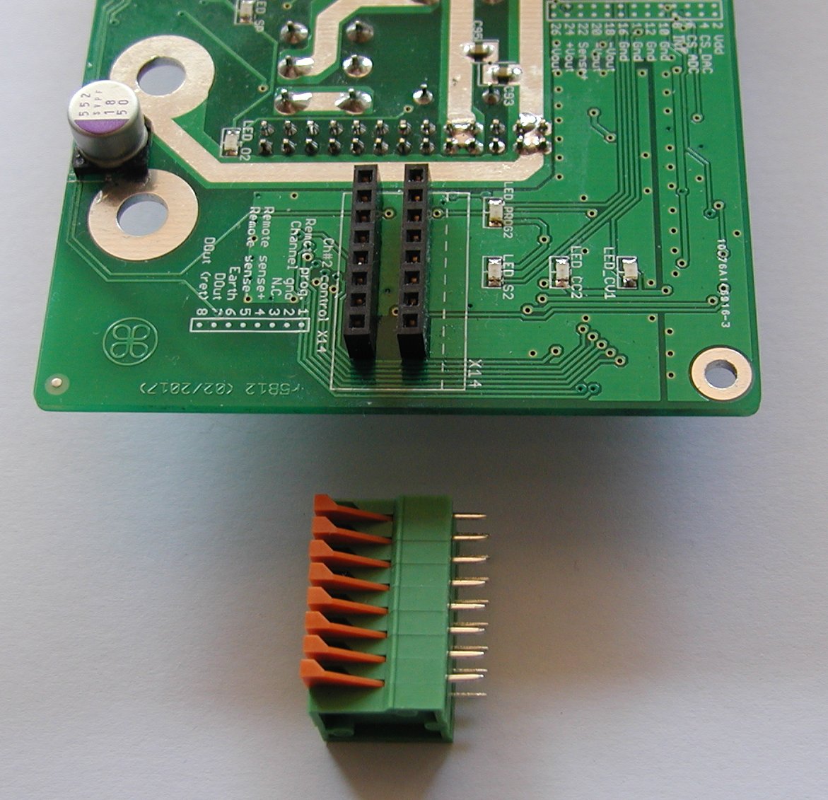
- Headers for Push-in connectors (X12, X14)
- 40-pin connector (LCD1) for the TFT touch-screen display
- Front panel power switch (SW1) and the incremental encoder (SW3)
Push-in connector distance adjustments
The distance (approximately 18 mm) between the rear side of the front panel and the Arduino Shield PCB is set by the TFT display height (or depth) when it’s fixed on the display mounting rail on one side and plugged in to 40-pin (LCD1) on the Arduino shield. It must be accommodated by the mechanical mounting of other parts.
The height of the push-in connectors (X12, X14) is about 13.5 mm, and when they are soldered directly on the PCB they will be 4.5 mm apart from the front panel surface. The pins will still be accessible, if only carefully. It’s more a question of visual appearance; a pair of low profile (5 mm) 8 pin sockets (example) anchor the connectors.
When all the SMD parts are mounted, followed by the THT parts, there are only a few parts left:
- The power relay must not interfere with mounting any of the surrounding parts (e.g. ZD7).
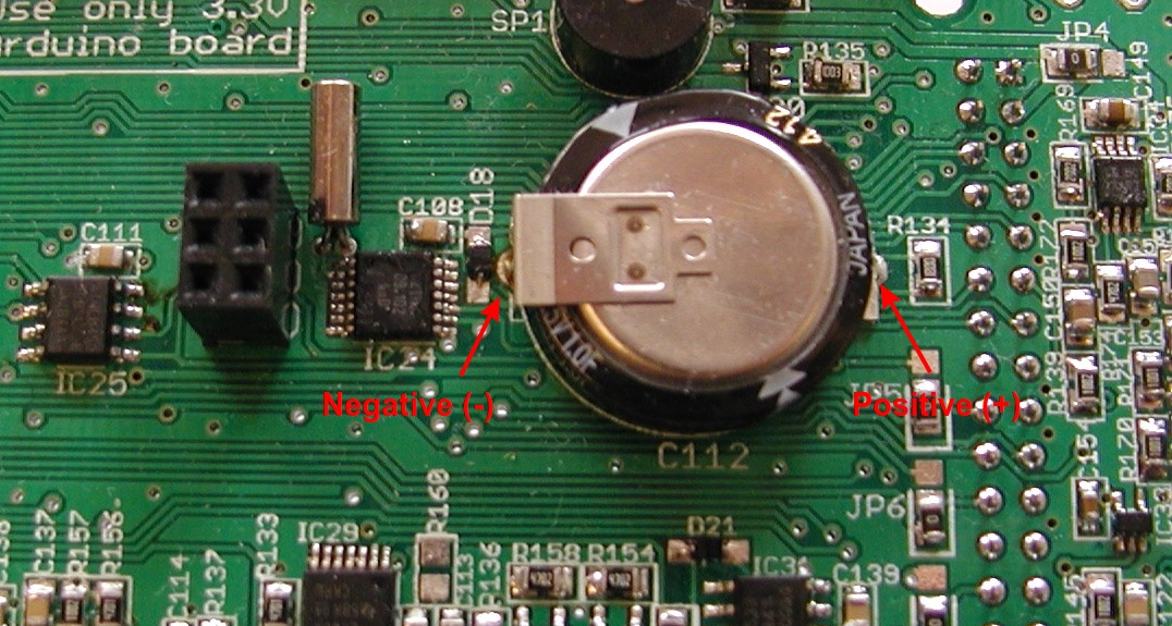
- The super capacitor is polarized, as are the electrolytic capacitors and the battery cell. Make certain all these are properly oriented, at least twice, before installing them! (see Fig. 5)
- If push-in connectors X12 and X14 are not yet inserted into sockets, as suggested above, then proceed with soldering them on the bottom side of the PCB.
- The TFT touch-screen display 40-pin connector (LCD1) has to be soldered on the bottom side too. To be completely sure it is aligned with the display, we recommend mounting the display on the display mounting rail and enclosure first, then inserting the connector on the display’s header, and finally place the PCB on top of the display. Then check the alignment of the PCB with the output binding post holes. Only when everything is in place can the 40-pin connector be soldered. Be careful as solder bridges between pins are easy to accidentally make in such tightly packed situations.
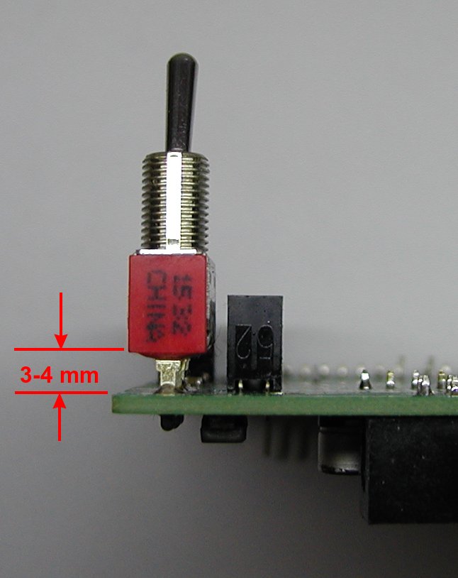
- Finally, we can mount the power switch (see Fig. 6). Once again, we recommended it be aligned with the corresponding hole on the enclosure’s front panel first, then adjust its position as needed before soldering.
Fig. 5: Placement of the supercap which backups the RTC chip – note the polarity, which must be correct.
1.7. Power board r5B12 assembly
The Power boards are the most complex parts of the PSU, given the number of components and the high currents it must handle. There are at least two possible assembly sequences: but in any case, be very disciplined and carefully solder all parts. Then simply plug it into the Arduino shield to check whether it will pass the self-test procedure. It does not require any special adjustment, and even when is not calibrated it should provide programmed output voltages and currents with good accuracy of which the PSU is capable.
The second possible sequence could be to assemble it in at least three stages:
- Power pre-regulator,
- Bias power supply and
- Post-regulator
After each section is completed, perform the simple testing procedure described below before continuing with the assembly. That way, you can limit possible damage if one section is mistakenly assembled (especially if bias power supply output voltages are wrong!).
WARNING: Never apply DC input (+48 V) when the AC/DC module is powered on (e.g., connecting cable manually to the X1 connector). That could generate a spike (due to L1) up to 100 V high that can easily destroy the on-board SMPS controller (LTC3864), even with ZD1 and C3 in place.
Power pre-regulator
The power pre-regulator circuit is shown on Sheet 1/12. We recommend you start with IC1 which requires soldering of the exposed thermal pad. A hot air soldering station instead of soldering iron probably should be used here. This section also require soldering L1 and X1 on the PCB’s bottom side . That should not be a problem if you are using a PCB holder. If you choose to supply the Power board with AC instead of DC input, follow Hack #1, and remember that any wiring connected to the mains must be handled with great care.
Once again, mount all of the smaller parts first and than continue with the bulkier ones such as L2, C3, C12, C15, etc.
When everything is soldered in place, you can proceed with basic testing. Since the board is not fully assembled, this requires some work-arounds. The first is to check whether the pre-regulator works properly. Q3 is used to enter the 100% duty cycle when the pre-regulator is bypassed. IC1 is then effectively switched off, and instead of the switching frequency a DC signal will be present on Q1’s gate (hence the name 100% duty cycle). But, we need to test whether switching works or not. There are two possibilities here:
- To apply +5 V (use some external source in this stage) to Q3 gate by soldering a thin wire (e.g. that used for wire wrap) to that position or
- simply place a zero-ohm resistor on position R14. Note: don’t forget to remove it before start testing the Post-regulator section and IC8 is mounted.
Before we can apply input power we need to provide some signal to the OUT+ trace. The easiest way is to locate any of pins 23 to 26 on the X2 connector.
Again, an external regulated source is needed. We can use the same +5 V used to turn on Q3 or something else with output of up to +40 V. In fact, we can start testing by simply connecting OUT+ to the ground. If OUT+ is grounded we can check, with an oscilloscope, two points to see if the pre-regulator works:
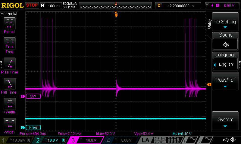
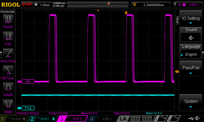
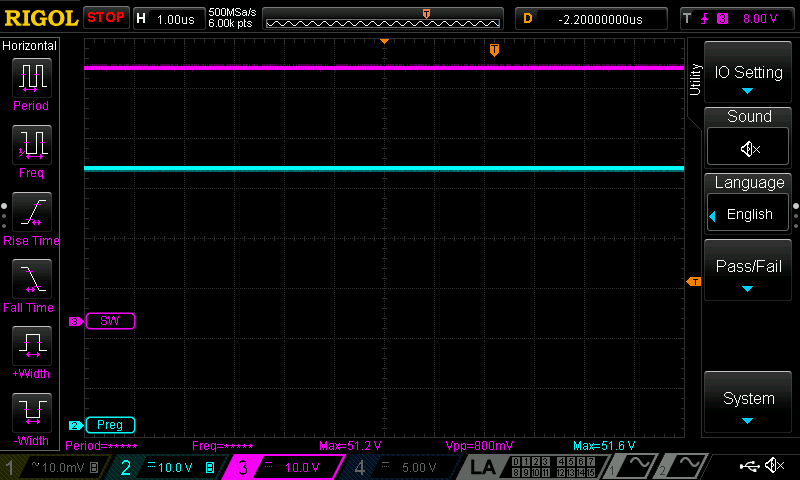
- The first is a “hot-spot” (SW, magenta trace) where Q3’s drain, the power inductor L2, and D1’s cathode are connected. Use an oscilloscope probe set to x10.
- The second test point is PREG_OUT (Preg, cyan trace), which is the output from the power pre-regulator.
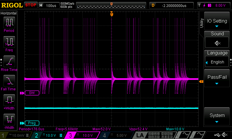
Fig. 7 shows the correct measurement when OUT+ is set to 0 V (i.e., grounded). Its output voltage will vary depending on the connected load and the difference between post-regulator output and power pre-regulator output. The voltage difference could be about +6.5 V for no load, to less then +3 V for full load of 5 A. Fig. 8 is another example (with no load) when +5 V is used for pre-regulator’s output voltage programming (measured PREG_OUT is +10.8 V).
Please note that in both cases the SW signal looks erratic only because no load is connected. Fig. 9 shows the characteristic switching pattern when a load is connected (e.g., a 10 Ω power resistor).
Finally, Fig. 10 shows what will happen if Q3 is not turned on. IC1 will enter a 100% duty cycle because the values for the voltage divider in the feedback loop (R13, R16) will be set well over pre-regulator input voltage, to +56 V, while the input voltage is no higher then +50 V.
The Low noise operating mode will remove some hard to filter switching noise from a channel’s output, when the pre-regulator works with a 100% duty cycle. But working in that mode puts real limitations on PSU output power, and if the PSU will be used for an application where higher output ripple can be tolerated, it’s possible to disable this option by removing Q3 and permanently mounting a zero-ohm resistor in position R14.
Bias power supply
Sheet 2/12 has to be followed to assemble the bias power supply circuit. As in the case of the power pre-regulator, start with IC4 which has an exposed thermal pad and will probably require a hot air soldering station.
When all other parts are in place, proceed with basic testing. Please note that the power pre-regulator will be now also powered up, and make sure that no load is connected to the PREG_OUT, perhaps leftover from the previous testing. Obviously, the first thing to test are output voltages at points +V and -V (IC4 outputs) and +5V (IC2 output). They must be within 5 % tolerance of +5 V, -5 V and +5 V.
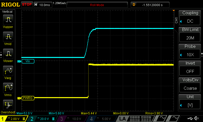
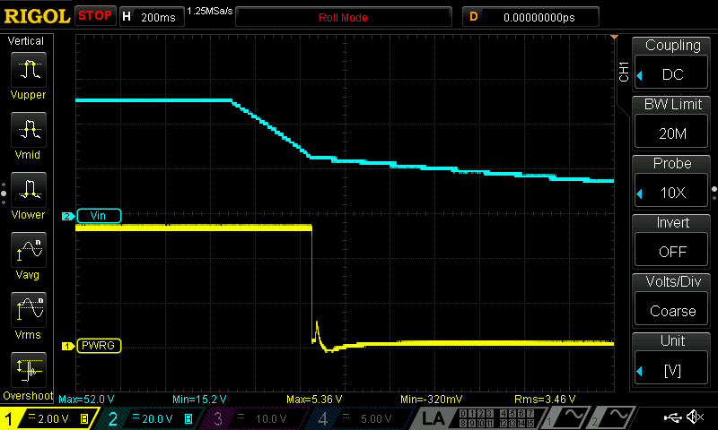
Another point of interest is PWRGOOD (IC2). It’s interesting to see how PWRGOOD relates to change of input voltage. That signal will be actively monitored by the microprocessor (MCU) and it will put the PSU into Stand-by mode as soon as possible when changed from high to low level. Fig. 11 and Fig. 12 shows the transition when input power is applied and removed.
Post-regulator
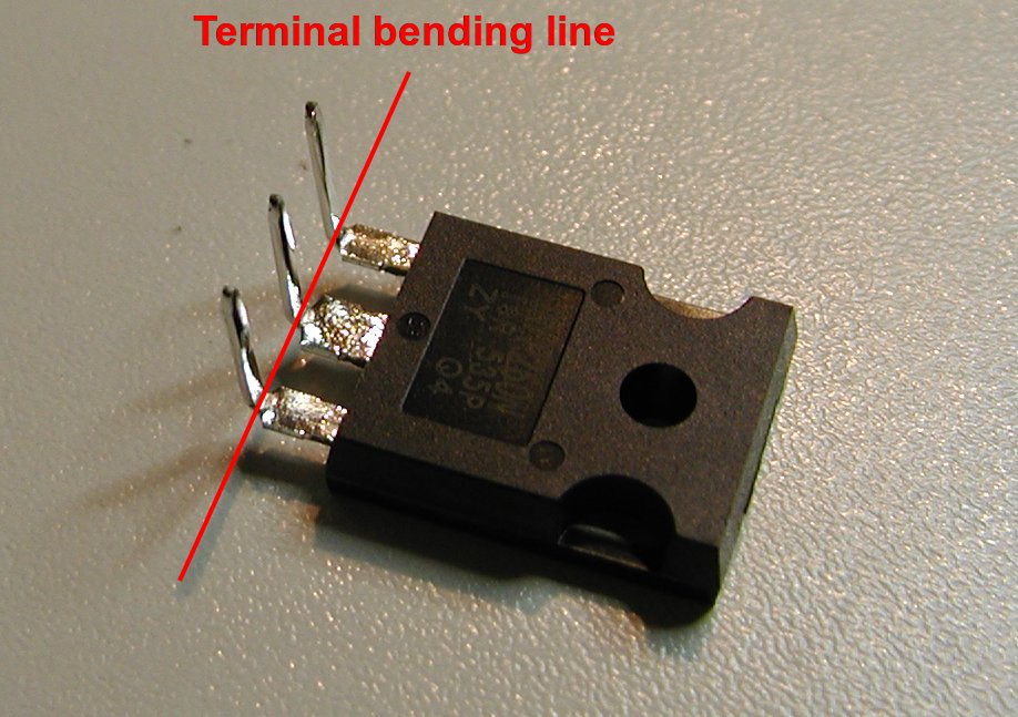
The post-regulator circuits are on Sheets 3/12, 4/12 and 5/12. The power MOSFET (Q4) requires special attention. It’s a THT part, and before soldering, its terminals must be bent (carefully, as they are often more fragile than you might expect) as is shown on Fig. 13.
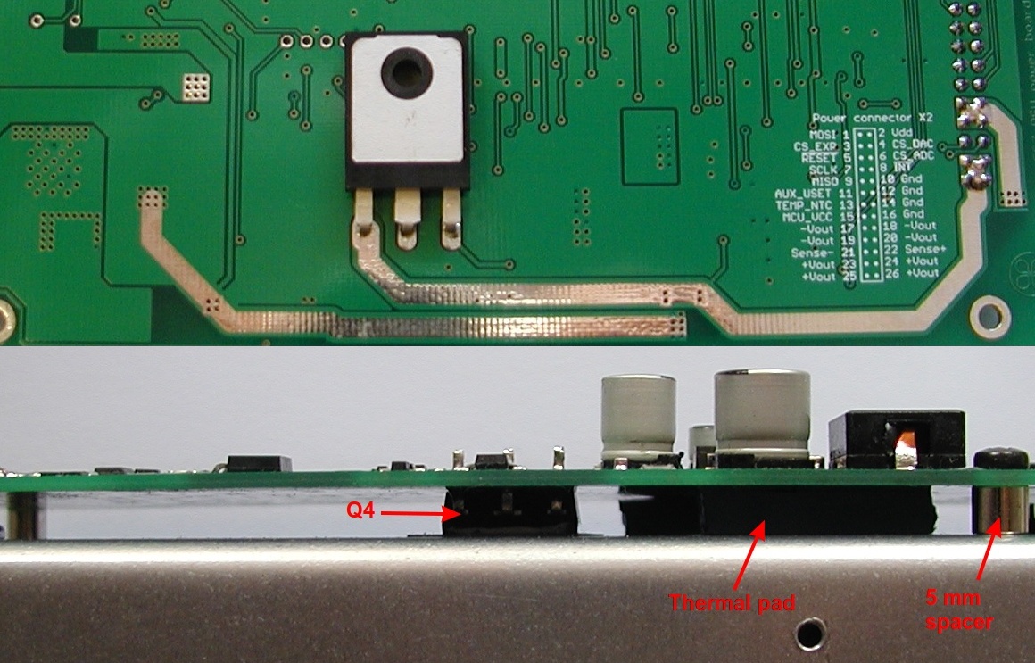
Q4 is mounted on the PCB’s bottom side, and if the EEZ H24005 customized enclosure is used, ensure that the distance between its surface area and the PCB’s bottom side is 5 mm. The easiest way to accomplish that is to mount the PCB on the heatsink (Fig. 14) using spacers, then mount Q4 (do not forget insulation!), fix it with a M3 screw and then solder it.
We highly recommend using a piece of 5 mm thick silicone thermal pad below the power pre-regulator area (IC1, Q1, D1) and high voltage LDO (IC3) (one source for small pieces at a reasonable price is AliExpress) as shown on Fig. 15. The temperature of a power assembly, as measured by NTC1 can be lowered significantly; as always, lower part and assembly temperatures during operation is quite desirable for part longevity and stability. Lowering the temperature will also affect cooling fan operation which will work with lower, quieter, speeds.
Do not use a metal block (with an insulation layer to prevent shorting) instead of the suggested silicone thermal pad since it could increase EMI (electrically related high frequency noise).
When everything is mounted, check a few points before connecting it to the Arduino Shield. Do not proceed until these values are correct.
|
Signal |
Value |
Position |
Comment |
|
+VREF |
+2.5 V |
IC9 |
Defines overall precision |
|
+OUT |
around zero |
Pin 23-26, X2 |
|
|
CV_ACTIVE |
+5.1 V (i.e., logic high) |
R84/R88 |
CV mode active (if U_SERVO is negative) |
|
CC_ACTIVE |
+0.6 V (logic low) |
R97/R99 |
|
|
POST_OE |
+4.67 V (logic high) |
R55 |
Output is disabled |
|
U_SERVO |
-1.1 V |
D7 cathode |
|
|
I_SERVO |
+0.28 V |
D9 cathode |
|
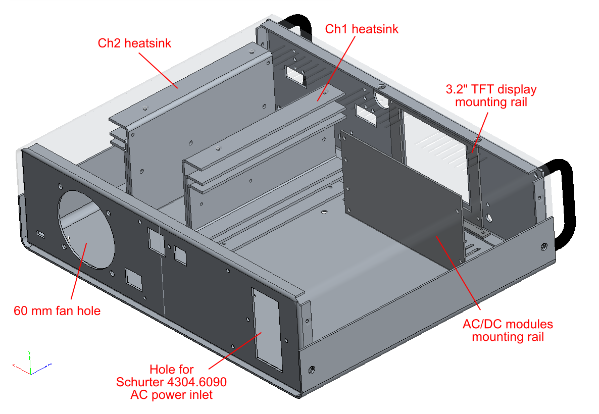
The next step, when all PCB modules are assembled and tested should be wiring and then installing them into the enclosure. The customized metal enclosure, manufactured by Varisom, has the following features (Fig. 16):
- Top and bottom plate with ventilation holes
- Front panel for TFT touch-screen display, binding posts, push-in connectors, light pipes (example) for LEDs, etc.
- Rear panel for AC inlet, DOUT2, USB, Ethernet, cooling fan and AUX PS module mounting holes
- Two set of three U-shaped aluminum heatsinks with Power module mounting holes
- Mounting rail for AC/DC power modules (Fig. 31)
- Mounting rail for TFT touch-screen display (Fig. 18)
- AC/DC module terminal cover (Fig. 32)
The wire harness specification is available in a separate section (link) which also includes the BOM. That specification is just an example how wire harness can be done, and users are free to use wires of different type and length, but only with equal or bigger diameter and voltage rating in the case of power paths.
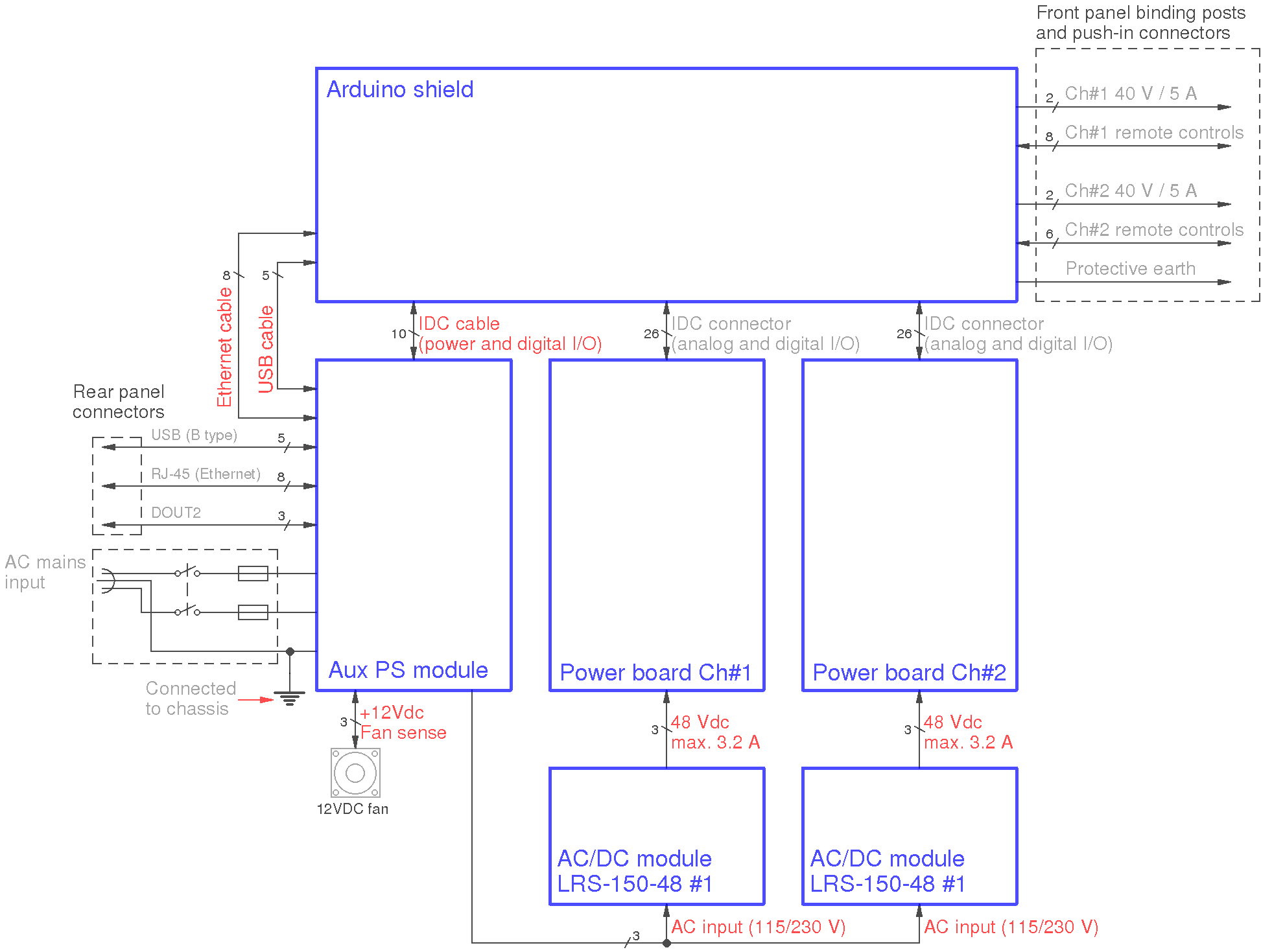
Two cables, one for USB connection between the Arduino board and the AUX PS module, and another IDC 10-pin flat cable for powering the Arduino shield are available assembled. All other cables must be cut to size and equipped with the appropriate connectors. It is important, most especially for wires and connectors carrying mains AC current, that the connections be fully insulated (heat shrink tubing is the usual choice); this reduces chances of an inadvertent short or any contact with a human. Good quality crimping and wire cutting tools are expensive, and if you already don’t have them a good choice might be the following:
- Jokari No. 20050
- Engineer Crimper with No.12 and No.13
Fig. 17 Shows a block diagram that should make clear how the wiring must run.
2.1. Front panel mounting
The Arduino Shield is mounted directly on the enclosure front panel and is fixed at six points: five binding posts and the 40-pin TFT touch-screen display connector.
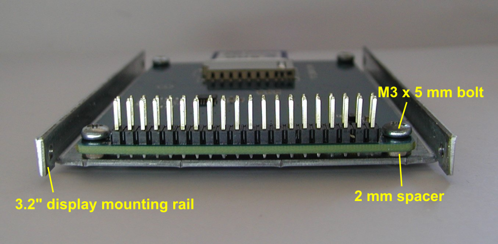
The 3.2” TFT touch screen display has to be mounted first on the display mounting rail as shown on Fig. 18.
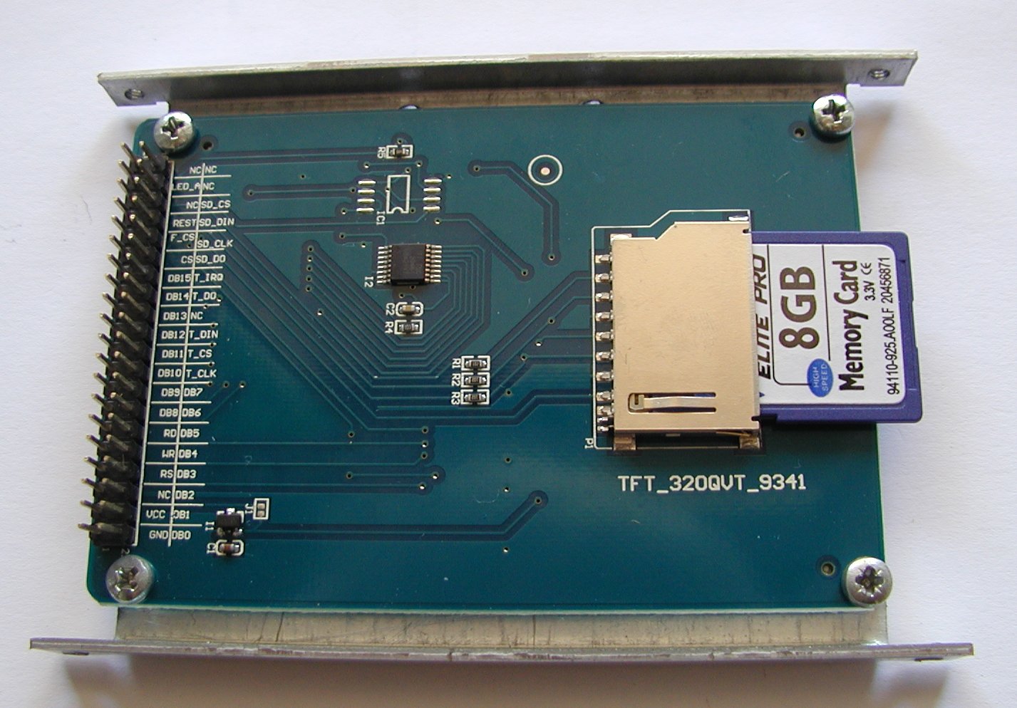
Before mounting the display rail equipped with the TFT display, a SD card must be inserted into the socket (Fig. 19).
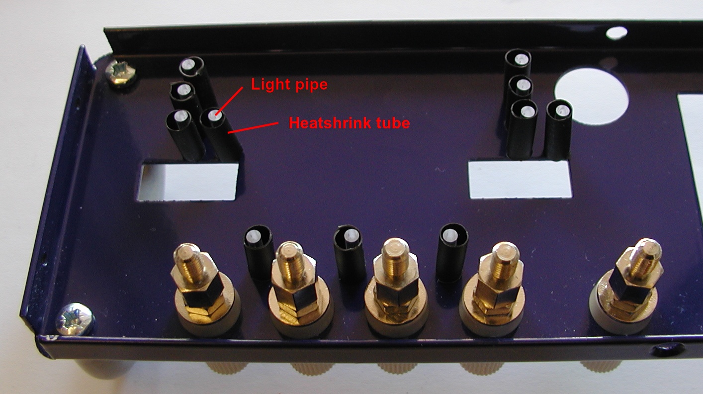
All LED indicators are mounted directly on the PCB bottom surface, and light pipes must be added so their lights will be visible at the surface of the front panel. Since we’ve included no separators between the LEDs, for best effect each light pipe should be masked with heat shrink tubing as shown in Fig. 20. Black is a good choice, for least spillover between them.
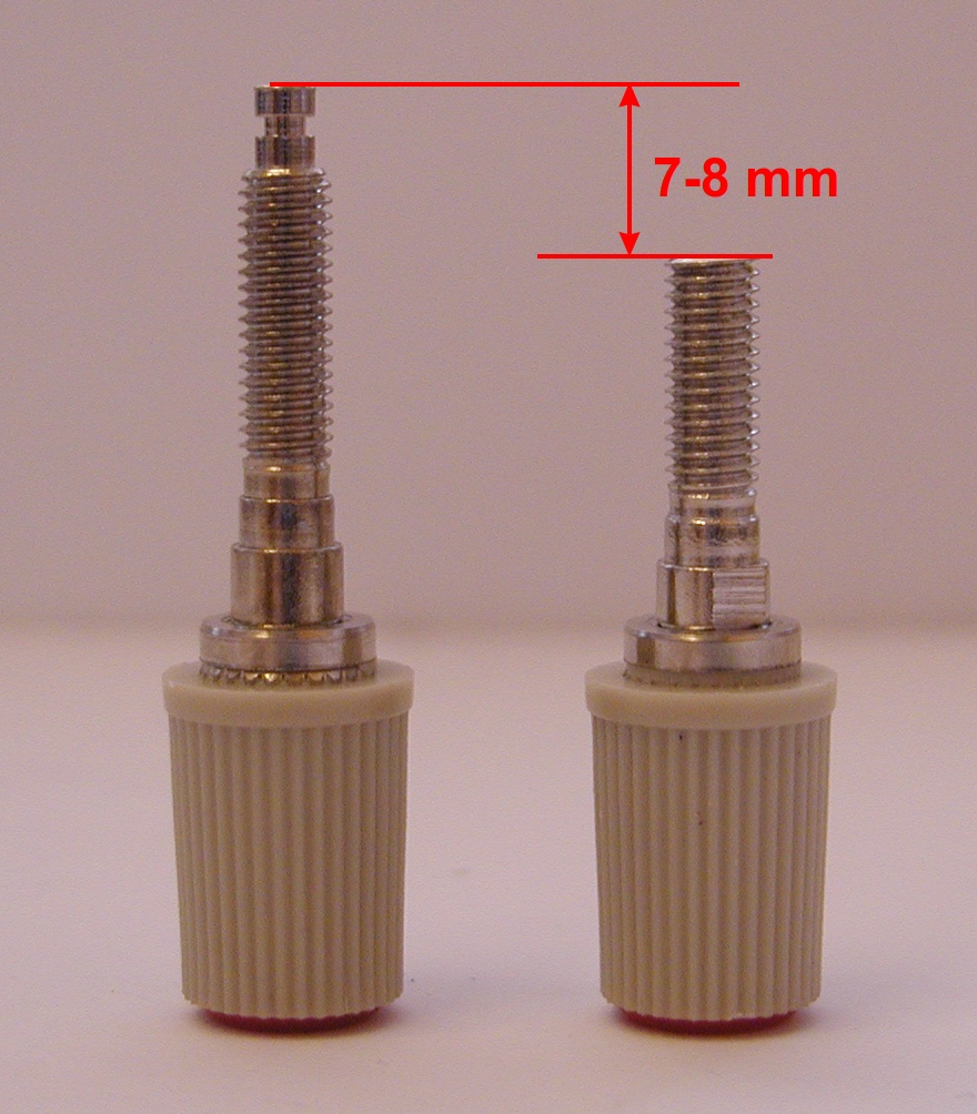
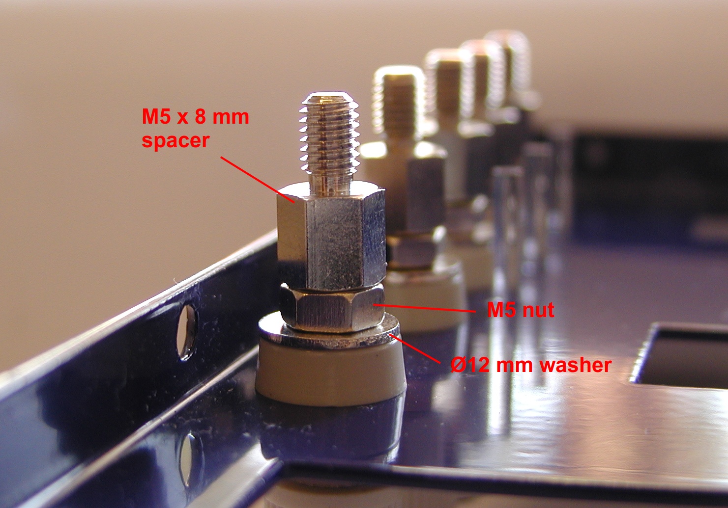
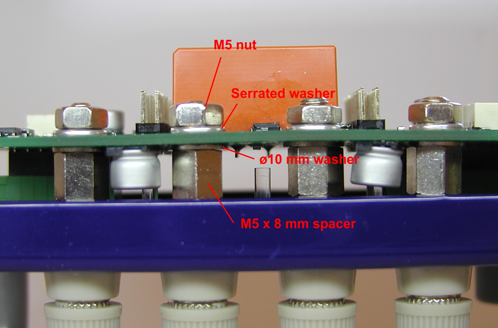
The specified binding posts are, simultaneously, too short and too long. They can short the PCB’s power outputs and protective earth to the front panel. It’s too short in that a nut with washer can be mounted on PCB’s top side. Therefore some kind of spacer is needed. But, if an 8 mm spacer is used it becomes too long and it has to be cut as shown on Fig. 21.
Binding posts comes with two M5 nuts, Ø10 mm and Ø12 mm washers that can be used while mounting it on the front panel (Fig. 22) and PCB (Fig. 23). It is important that locking washers (preferably the serrated, toothed sort) are used to prevent the binding posts from becoming mechanically loose. Using a small amount of threadlocking fluid is probably a good idea.
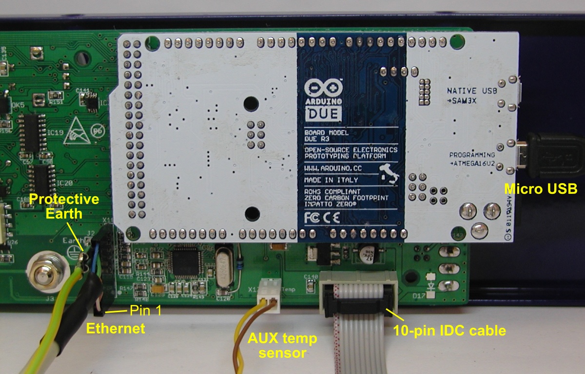
The Arduino Due board should be inserted before the Arduino shield PCB is mounted on the front panel. Cables as shown on Fig. 24 must be inserted before the front panel is mounted to the enclosure’s bottom plate.
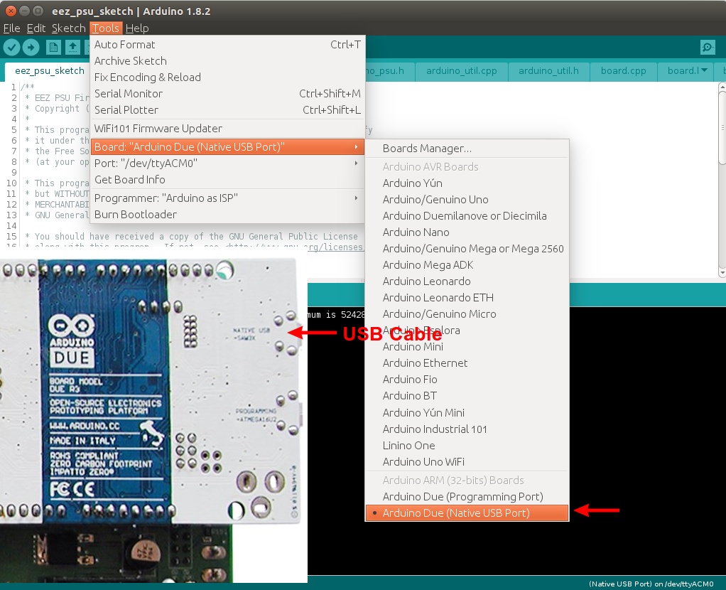
Please note that from firmware v1.01. the default USB port is Native not Programming.
2.2. Rear panel mounting
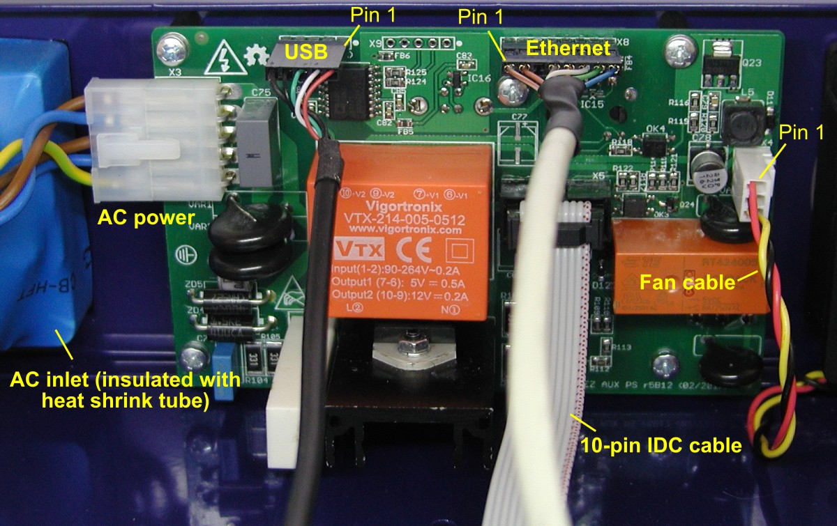
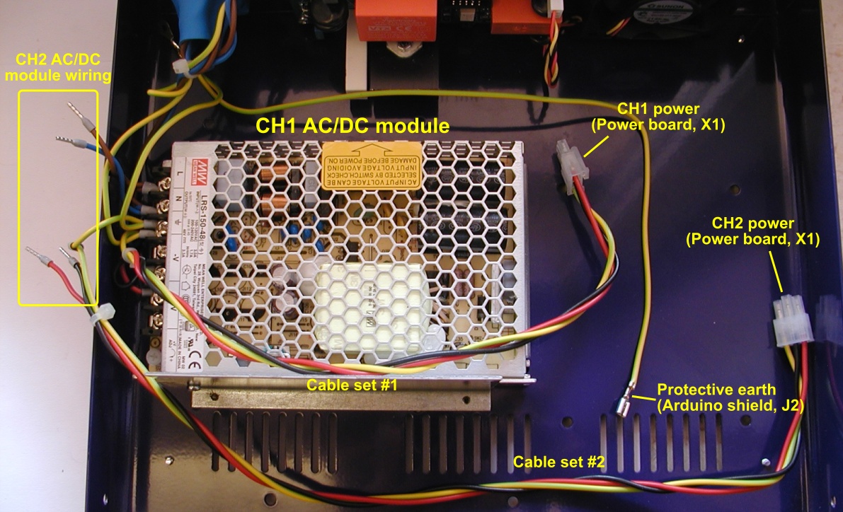
When the assembled and tested AUX PS board is mounted on the enclosure’s rear panel using five M3 bolts and 14 mm spacers, it will be connected with other parts and modules using five cables as shown in Fig. 25.
WARNING: pay special attention when connecting the Ethernet cable. Wrong installation is likely to permanently damage the RJ-45 modular jack (X7).
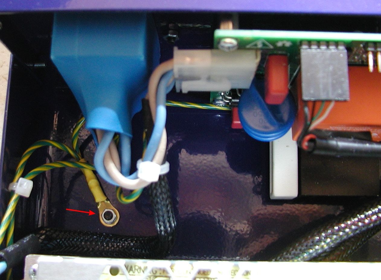
The various protective earths from the PCBs etc. MUST be connected very securely to a single point on the metal enclosure as shown in Fig. 26. Any violation of this rule will almost certainly increase noise and hum within the PSU and quite possibly interfere with PSU operation. Make certain that the ring terminal (or terminals if you use more than one) makes good electrical contact with the enclosure by using an externally serrated washer (example). Make certain the earth connection bolt has been properly tightened so that it cannot, and will not, become loose. Using some threadlocking fluid is a good idea here, for proper grounding is important to correct circuit behavior. The earthing requirement (which might affect mounting details) may vary from country to country, since the safety earth is often a legal or regulated issue; therefore please check for what is required, or prohibited, in your location.
2.3. AC input selection
WARNING: take precautions when working with AC mains voltages. There is a possibility of exposure to lethal voltages and currents if there is an error. Too much care is probably not possible.
There are options for providing the PSU with AC mains voltage. It is possible to feed AC directly to the power boards using a mains power transformer (and rectifier bridge and filter capacitors as described in hack #1), or, as the basic design assumes, some switching power supplies. These choices dictate fuse ratings and other issues. In general, the mains fuse current rating must be twice the correct value when using 115 Vac then when using 230 Vac (more current at the lower voltage to carry the same power). We have used 4 A fuses (example) for the two LRS-150-48 switching power supply modules (the maximum combined output power is 320 W and, with the listed 90 % power efficiency, a minimum fuse of 3.13 A is required). Two fuses are needed when an IEC standard input connector such as Schurter 4304.6090 is used.
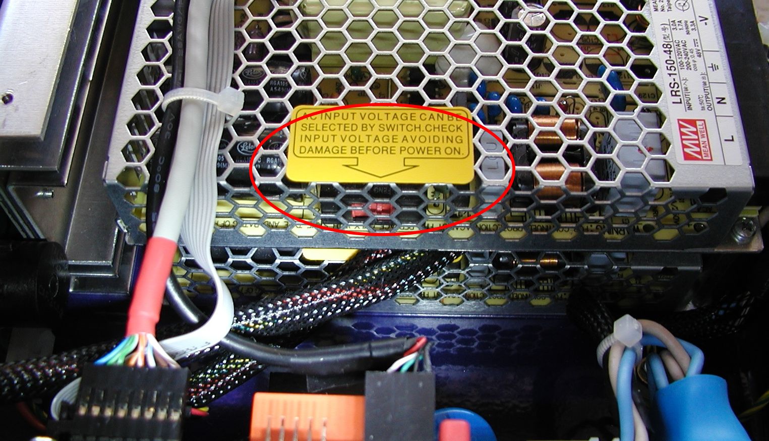
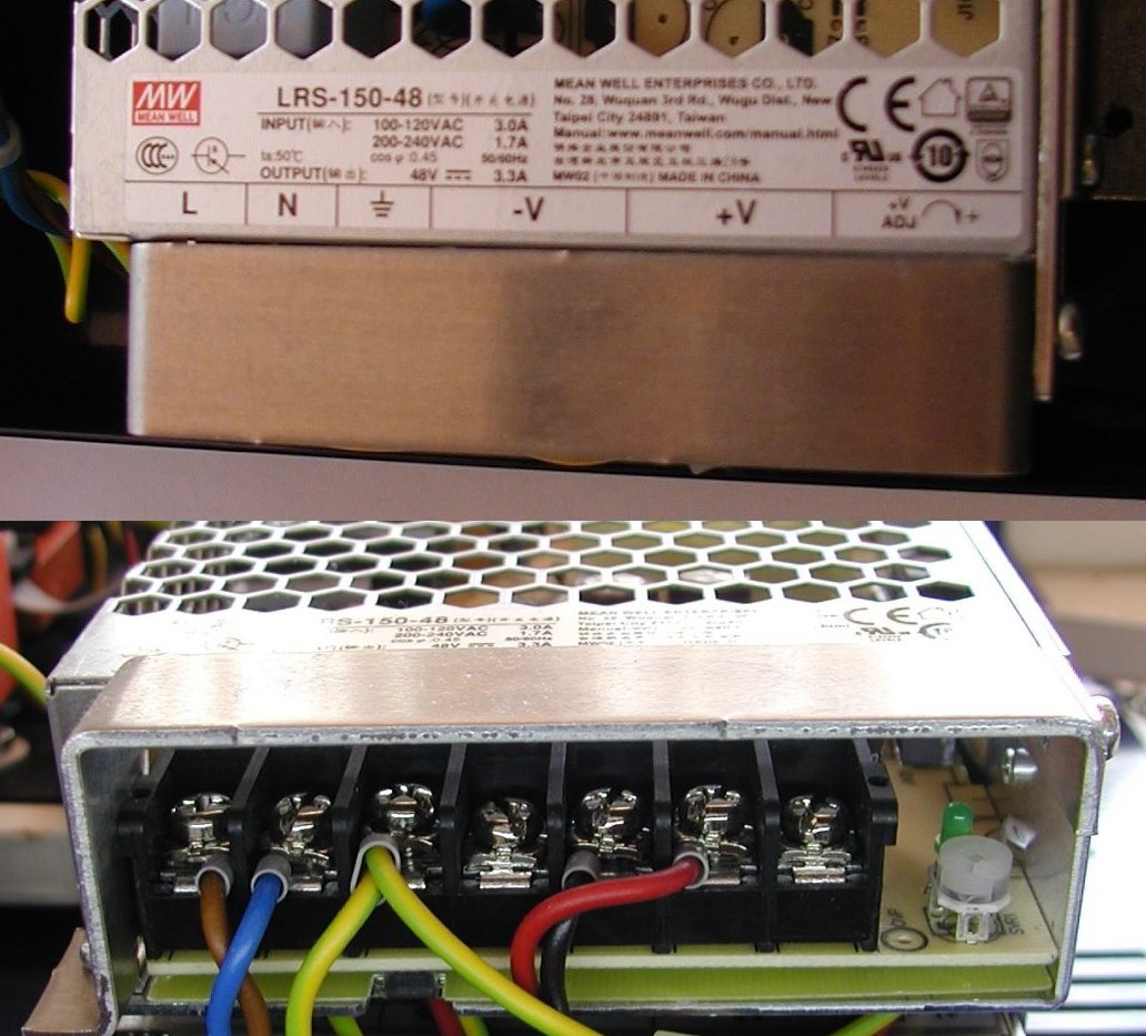
AC/DC switching power modules often come with or without automatic input voltage range adjustment. When a manufacturer offer two models with the same output ratings, the model without that feature is usually a little cheaper. For example, the LRS-150-48 comes without the auto-range feature and has a manual switch (Fig. 27.) to adjust for different AC input voltages. That switch is not easily accessible when those modules are mounted inside the enclosure, so make certain that switch is in proper position before mounting and AC mains voltage is applied. When moving to an area with different mains voltages (e.g., 115 Vac to 230 Vac) these switches MUST be changed appropriately and back again when returning.
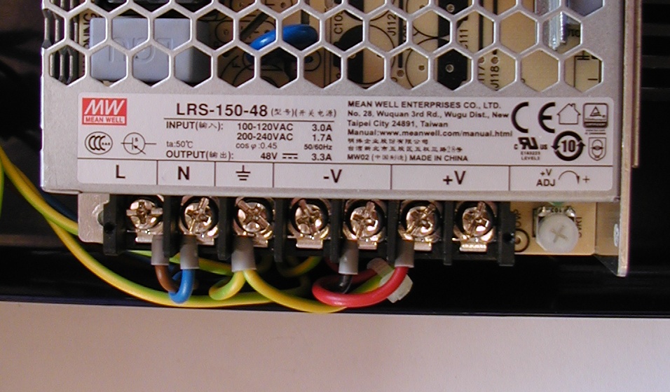
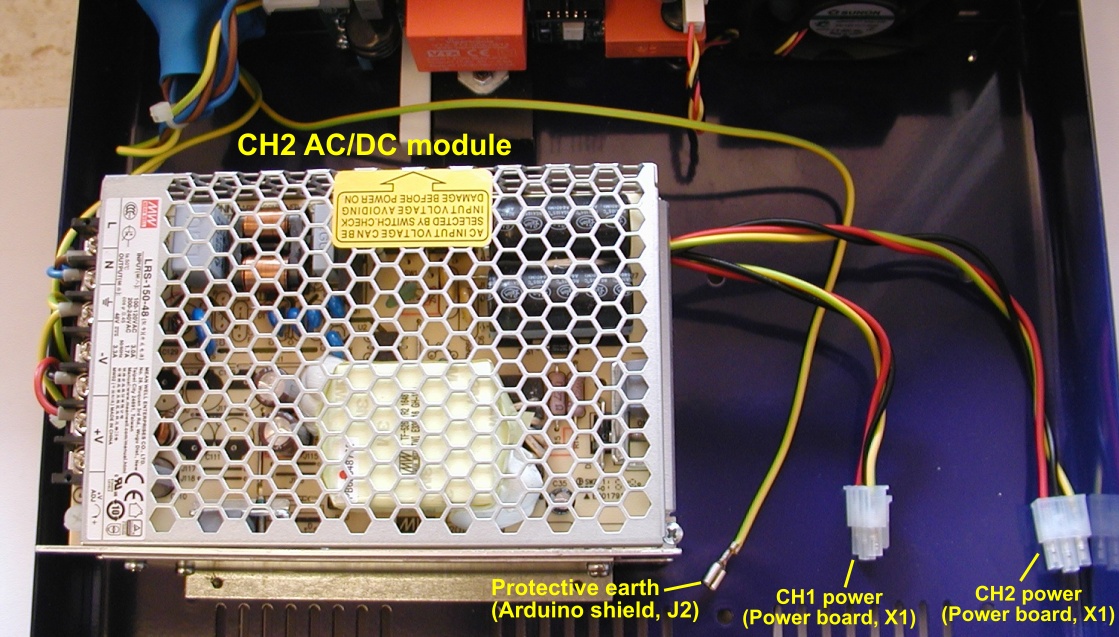
Cable set #1 and Cable set #2 are connected to the both AC/DC modules using the wire colors as shown on Fig. 28:
|
Name |
Position |
Color |
|
AC line input |
L |
Brown |
|
AC neutral input |
N |
Blue |
|
Protective earth |
|
Yellow-green |
|
DC output negative |
-V |
Black |
|
DC output positive |
+V |
Red |
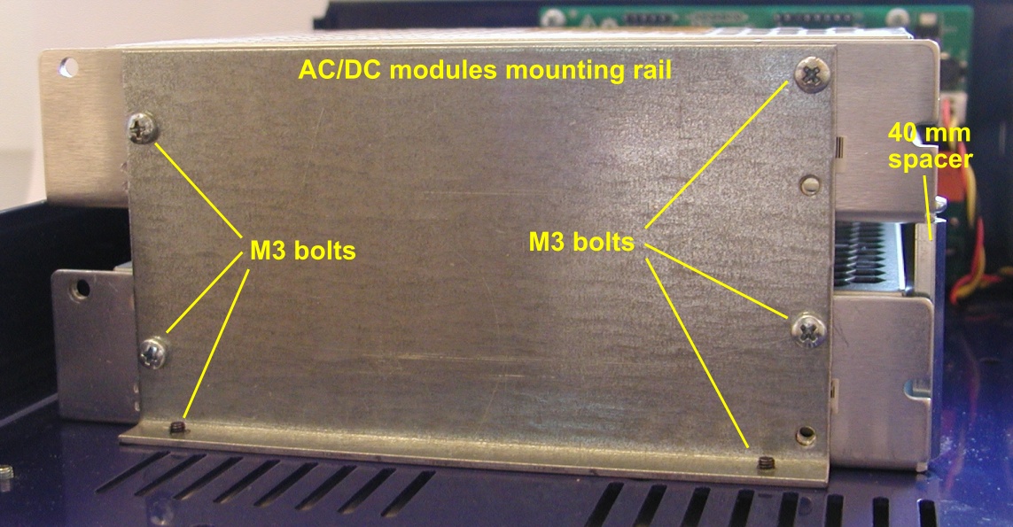
The two AC/DC modules have to be stacked on top of each other and mechanically fixed on one side with the AC/DC mounting rails (Fig. 31). Those bolts hold equipment with AC mains current connections; it would be well to use a little threadlocking fluid on their threads to prevent accidental loosening. Additionally, two 40 mm long spacers are used for better mechanical strength.
Finally, an AC/DC module terminal cover should be mounted as an additional protective measure (Fig. 32).
The PSU is controlled by an Arduino type board which also runs the display. The correct version of the software which runs on the installed Arduino version must be installed in non-volatile memory within the MCU. This can be done in the field, and revised as new versions of the software are released.
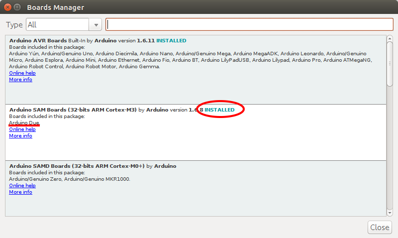
Compilation and uploading to the Arduino Due board (mounted on the Arduino Shield) requires that users install and run the cross-platform (Windows, Linux, etc) Arduino IDE program which can be downloaded here. Installing the Arduino IDE alone is not sufficient in the case of the recommended Arduino hardware version since support for ARM boards such as the Due is not installed with the IDE download by default. Therefore you have to add ARM Cortex-M3 support. Navigate to Tools… Board:… Boards manager and select the Arduino SAM Boards package for installation. When it’s successfully installed, you can check for it as shown in the Fig. 33.
The next step is to select the particular Arduino Board installed in the PSU (there are many variations) and USB. The Arduino Due board has several advantages, not least of which is that it has two USB ports. We’ll use Native Port as shown on Fig. 34.
After successful installation, the Arduino IDE is ready to use and we can continue with downloading firmware from the GitHub repository for this PSU. Note that the r5B12 board versions require firmware revision M4 or newer (found in the Releases section).
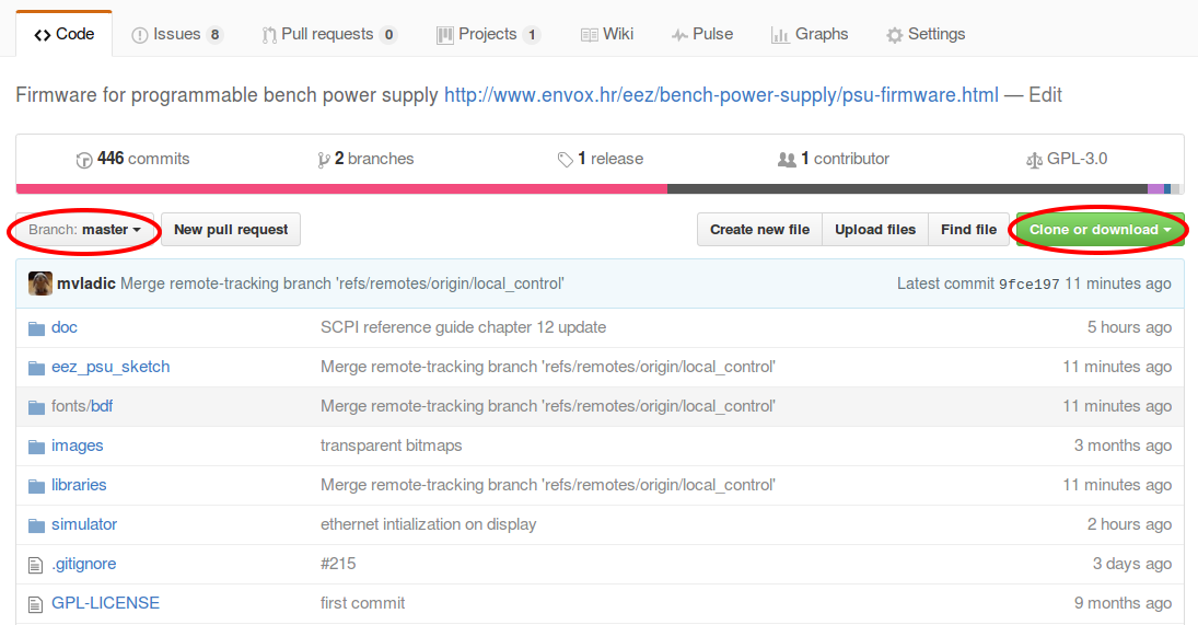
Another possibility is to use the most recent build that can be found in the Master branch. In that case, move to the Clone or download option and select Download ZIP option to save the latest build on your PC as shown on Fig. 35.
Additionally you have to download library for Ethernet controller that can be found here. Otherwise you can expect error while compiling (that issue is addressed in GitHub issue #159).
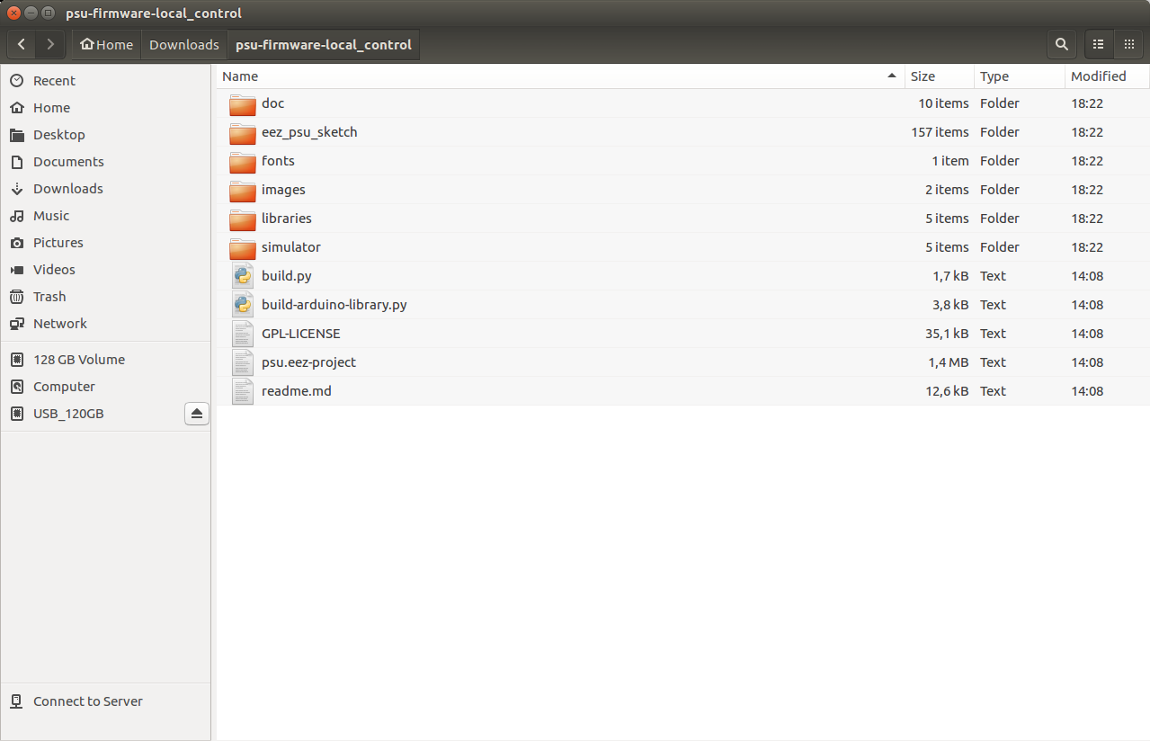
When the zip file has finished downloading, extract the files in the master.zip package. The following folder tree should be created:
The two folders will be used to compile firmware within the Arduino IDE: eez_psu_sketch and libraries. The contents of the latter one must be copied into the Arduino folder containing 3rd party libraries. The directory (folder) needed will vary; it could be e.g. /home/denis/Arduino/libraries on Linux or My Documents\Arduino\libraries on Windows. See also this article.
The firmware upload require the following steps:
- Power up the PSU
- Make sure that no loads are connected on the outputs
- (Re)start the Arduino IDE
- Check that the correct USB port is selected under Tools… Port:
- Load the firmware program (i.e., an Arduino sketch) eez_psu_sketch.ino (File… Open)
- Start the upload (Sketch… Upload or select the Upload icon on toolbar)
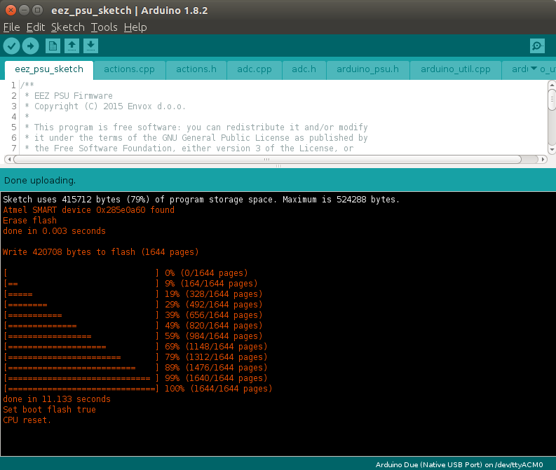
- While the upload procedure proceeds, a progress bar will appear (Fig. 37).
- Reset or restart the PSU if necessary
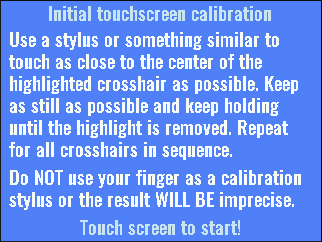
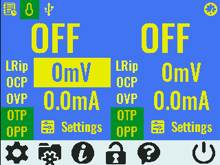
On first start after the firmware is properly installed, the touchscreen calibration page (Fig. 38) will be displayed; you must not skip this test since without a calibrated touchscreen interaction could be erratic or even impossible. Thereafter, a welcome page (Fig. 40) will be displayed for a few seconds when the PSU is turned on.
When the initial touchscreen calibration is finished, the self-test will be started. Passing it is a good indicator that MCU control over all circuits has been established. If the self-test is passed, no additional message will be displayed, and the firmware will proceed with the main page (Fig. 40).
A work in progress
Simple building instructions and firmware upload for EEZ H24005 programmable power supply.
| 1 | ^Solder comes in solid forms (generally used for such things as plumbing), and in wire with embedded soldering flux. In the last case, that flux must be compatible with electronic parts; use of acid core or acidic paste flux damages electronic parts and PCBs. The usual embedded rosin core flux types are R, RMA, or RA, in increasing order of activity, with RMA being a good general purpose choice. Organic flux (typically denoted as water soluble) is still more active and, like RA, must be removed after soldering lest PCB traces or joints be prone to failure. Solder paste can be used for SMD parts and those with exposed heatsink tabs, but don’t forget that solder paste is not easy to apply by hand, can be messy, and in the best case has a very limited shelf life even when refrigerated; use only a small package, example). The purpose of flux, in all cases, is to chemically clean the surfaces being joined; dirtier and more corroded surfaces require a more active flux to get a good solder joint. Also, note that soldering is not welding, in the sense that the process does not physically and mechanically meld two items. Solder does not dissolve into the surfaces, at least not usefully. Even a good solder joint has little mechanical strength, and two wires, for instance, must be folded back on each other to provide the strength needed. The solder, even in a proper good joint, will not. Soldering is useful only to make electrical contact, and would be improved if it were transparent, for a solder joint may look acceptable but be electrically inadequate due to invisible voids or poor wetting. Solder wets a properly prepared surface when it makes a good joint, and the presence of smooth margins around a solder joint is an indication that this wetting has occurred. Many constructors will already know this, but it may help to point out some of the oddities of solder composition. As used in electronics – for a long time – solder was a mixture of lead and tin (plus, rarely, small amounts of other metals, such as silver). The special composition 63% tin / 37% lead, is called eutectic, and has the property of having a definite melt / solidify temperature, which is the lowest of any tin/lead mixture. 60/40 solder is close, and is more common, but like all non-eutectic solders doesn’t have a definite melting point, getting more and more mushy as the temperature increases; the official term is plastic region. It is harder to tell just when the joined parts have been properly wetted, and sufficiently cooled that inadvertent small motions will not compromise the joint leading to eventual failure. Concern over health issues due to lead content in solders has led to the RoHS regulations, originally in the EU, which are designed to remove lead from solder. Compositions of conforming solders vary, but most include tin as well as some silver, antimony, etc. None has a melting temperature as low as 63/37 eutectic solder, all seem to have an extended plastic region, and all require much higher temperatures. Use of a vapor ‘extractor’ is a good idea in any case; these are a small fan with an attached filter which disperse, and ideally absorb, soldering fumes (nearly entirely from the flux used), reducing the amount available to be breathed into lungs; some even have built-in lights. Flux vapor contains a considerable variety of unpleasant and incontestably dangerous (in sufficient concentration) chemicals. It is fortunate that soldering releases only small amounts. Metal contamination (e.g., by lead particles) is largely confined to hands and fingers, so touching eyes or nose whilst soldering is to be avoided. And, wash hands thoroughly after a session at the bench with the soldering iron to avoid food or drink contamination. Lead really is a very significant toxic material, in very small amounts, especially neurotoxically. |
| 2 | ^The most common form is part water and part alcohol – avoid those with additional ingredients such as perfume or oils – higher alcohol concentrations are more effective in dissolving and removing flux residue. Extra stuff will often leave a different residue on the board example, and paper wipes example for cleaning (the microfibre sort leaves much less fluff and fiber bits behind. Common paper towels for kitchen use are not very useful). More aggressive chemicals for flux residue removal include acetone, and lacquer thinner. All of these very flammable and quite dangerous – especially the last two – so make very certain there is no ignition source in the vicinity (a hot soldering, a lit cigarette, or an electric heater, or switches or relays all qualify, as do invisible commutation sparks in normally operating large (or very small) motors – heaters, water pumps, air conditioners, fans, …). In fact, cleaning PCBs of flux residue is best done outside of a structure, in the open air and, ideally, with a light and refreshing (and dispersive!) breeze. Use the smallest amount of cleaning fluid possible. |
| 3 | ^If they get spilled anyway, an LCR meter can help sort them out. Many DMMs don’t have a capacitance measurement feature, and of those which do, still more are just barely adequate. There are some fully satisfactory and inexpensive meters (usually called transistor testers) available on the Internet, built around an Atmel microcontroller, and based on an open source design from Germany. At this writing, those built around the 328 chip (firmware version 1.12 or later) are known to work well. They are usually more awkward than a purpose built LCR meter, and may not accommodate as wide a capacitance range as you need. On the other hand, purpose built LCR meters are more expensive, though they often support more precise 4-wire measuring techniques (i.e., Kelvin wiring) and can also measure resistance values too low for most DMMs. And inductors too! Unfortunately, they are not as well protected from mistake and unsuspected circuit conditions as is a good DMM, and so are not a generally satisfactory substitute. |

