Hacking area
There are a variety of custom changes available for the PSU. Some of can be done by simply adding parts that are marked as optional in the design documentation, others will require replacing existing parts. Additionally our (and your) ideas about further improvements will be also listed here.
- Hack #1 – Choose power input
- Hack #2 – Set output range
- Hack #3 – Disable the low ripple mode of operation
- Hack #4 – Remove Arduino powering over USB option (obsolete)
- Hack #5 – Isolate the USB port electrically
- Hack #6 – Communication ports protection
- Hack #7 – Use of an external W5500 Ethernet module (obsolete)
- Hack #8 – Improve high current range precision
The power board can be connected to DC as specified. Or the AC/DC switching power supply modules can be left out, and an AC power input connected to the PSU itself. For the planned EEZ H24005 AC/DC power supply modules were chosen. Therefore the DC from them is supplied to the PSU boards. If you got only the PCBs or the assembled versions, and not the complete kit, AND you happen to have an appropriate spare mains transformer you can use it instead. Construction requirements for a transformer options are really minimal – only one secondary winding per channel is needed. With the right output voltage and current/power you can (re)use it for a new bench power supply.
Mains transformer output must be connected to the AC input and a few additional parts are required. Note that this means that AC power will be present within the PSU in ways not covered in the standard PSU documentation, schematics, and photos. Take due care to ensure that opportunities for failures (shorts, loose wires, bad solder joints, and so on), and for electrocution are reduced to the minimum.
Here is what you need to do:
- Remove C1, C2, C4, L1, X1 if they exist on the Power boards PCB
- Mount THT parts X2, C145, C146 on the bottom side
- Mount on top layer SMT parts D22, D23, D24, D25, R168 and if you like ZD15
Caution: make sure that max. output voltage (Vmax) when rectified never exceed the absolute maximum rating of both IC1 and Q1. They will be permanently damaged. The limit is 60 Vdc which is just about 41.6 Vac. The power board has been tested with the Talema 55186-P1S2 mains transformer; the nominal output is 40 Vac.
Until the present, the EEZ PSU design has been tested with two output ranges: 50 V, 3.12 A and 40 V, 5 A. The later was selected for the EEZ H24005 model. If someone wants to use a non-standard power input e.g. 36 V, 100 W LED driver power module, or some smaller transformer then the one tested in #1 above, modifications to the CV and/or CC control loop gain will be required.
The gain of the CV control loop can be changed by substituting a different feedback loop resistor for IC5B. The maximum output voltage is reached when the drop across it is equal to the reference voltage; in the standard PSU design, that will be +2.5 V, provided by the precision voltage reference IC9. Therefore, for a default setup of 40 V we need a gain (actually an attenuation) of 2.5 / 40 = 0.625, which, when translated into fractional numbers gives us a rounded ratio of 5/8. Now we have to choose two resistor values with that ratio, and check to see if they will work using one of many online op-amp voltage and gain calculator which can be found here. A hand calculation is likely to teach more, however. One of the main obstacles here will be the required precision. You should choose at most 0.1% and a definitely a low temperature coefficient for acceptable results. The following table offers resistor names and values for two additional ranges together with the default of 40 V.
|
Range |
Required gain |
R43, R53 |
R44, R54 |
|
0 – 30 V |
0.08333 (5/6) |
75 kΩ |
18 kΩ |
|
0 – 40 V (default) |
0.0625 (5/8) |
100 kΩ |
24 kΩ |
|
0 – 50 V |
0.05 (1/20) |
130 kΩ |
24 kΩ |
The gain of the CC control loop depends on IC7A’s gain, but also on the current sensing resistor R65 that defines the voltage drop which can be expected for current flowing to the load. According to Ohm’s Law, it’s obvious that the voltage drop (U = I * R) will be higher, and we can expect better precision, for smaller currents. But that will also mean higher power dissipation for that resistor. For example with 200 mΩ we’ll get 1 V for a maximum range of 5 A, but power dissipation in that case will be 5 x 5 x 0.2 = 5 W which will be invitation to failure and fire. A constant dissipation of 5W is not at all easy to remove; it is therefore unacceptable. With a selected 20 mΩ resistance, it is 500 mW but maximum output is also ten time smaller at 100 mV. Again, as in case of the CV control loop gain discussed above, 100 mV has to be amplified to 2.5 V for a full scale reading. Therefore, the required gain will be 2.5 / 0.1 = 25. The following table offers two additional ranges together with the default one of 5 A.
|
Range |
Required gain |
R60, R70 |
|
0 – 3.12 A |
40 |
3.16 kΩ |
|
0 – 4.16 A |
30 |
2.7 kΩ |
|
0 – 5 A (default) |
25 |
1.91 kΩ |
The PSU firmware has to see operational changes on the Power boards, otherwise you the PSU will produce unexpected, and probably unacceptable, output values. The recommended place for all user code changes is conf_user.h file.
For example, we might want to expand the voltage range because we have found that when a channel is calibrated it cannot reach the maximum value, e.g. instead of 40 V, we get 39.95 V. This can be managed by changing the CV control loop gain (default, 0.625) by increasing R44, R54 to 24 kΩ to decrease gain to about 0.0615. In that case the maximum programmed value (for DAC output 0xFFFF) will be 40.67 V. The firmware constants of interest for 40 V, 5 A configuration are CH_PARAMS_U_40V, CH_PARAMS_40V_5A and CHANNELS.
There are two possible ways to configure the firmware to take care of our changes. The first is to simply redefine CH_PARAMS_40V_5A, by changing voltage range value from 40.0f to 40.6667f. Add the following lines in conf_user.h:
	#undef  CH_PARAMS_U_40V
	#define CH_PARAMS_U_40V    0.0f,  0.0f,  40.0f, 40.6667f,   0.01f,      0.1f,       5.0f,       0.15f,         19.1f,         38.0f,         25.0f,     CH_PARAMS_OVP
Another way is to introduce a new voltage parameter constant (e.g. CH_PARAMS_U_40.67V) and a new channel parameter (CH_PARAMS_40.67V_5A) that will be used to set new definition of both channels in CHANNELS:
	#define CH_PARAMS_U_40.67V    0.0f,  0.0f,  40.0f, 40.6667f,   0.01f,      0.1f,       5.0f,       0.15f,         19.1f,         38.0f,         25.0f,     CH_PARAMS_OVP
	#define CH_PARAMS_40.67V_5A             CH_PARAMS_U_40.67V, CH_PARAMS_I_5A, true, CH_PARAMS_OPP_DELAY,  0.0f, 155.0f, 155.0f, 48.0f, 2.2f, 25.0f, 160.0f
	#undef CHANNELS
	#define CHANNELS \
	    CHANNEL(1, CH_BOARD_REVISION_R5B9_PARAMS, CH_PINS_1, CH_PARAMS_40.67V_5A), \
	    CHANNEL(2, CH_BOARD_REVISION_R5B9_PARAMS, CH_PINS_2, CH_PARAMS_40.67V_5A) \
Hack #3 – Disable low ripple mode of operation
The Power board allows the MCU to shift to a low ripple mode. If this feature is not required or you are going to experiment with firmware that could potentially introduce some disturbance in limiting output current and power (beware, Q4 could be damaged in that way), then you can permanently or temporarily fix that by disabling it on the Power board directly. All what is needed is the following:
- Remove Q3
- Mount R14
Hack #4 – Remove Arduino powering over USB (Obsolete)
This hack is limited to the Arduino Shield r1B9
The Arduino Shield carries the Arduino board used for digital control of the PSU. The Arduino board is also powered with 5 V via the Arduino Shield (from the Auxiliary power module). But some Arduino boards are designed to be powered also from a connected host PC via USB port. Therefore, if a USB cable is connected to the PSU, the Arduino board will stay powered even if the PSU is disconnected from the mains voltage. Which will make SW1 on the front panel effectively unusable.
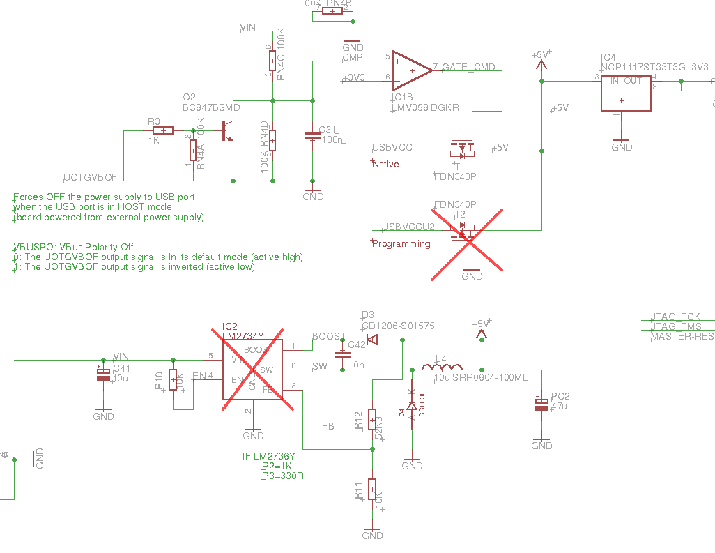
If this behavior is unacceptable, it can be easily fixed by removing MOSFET T2 (see Fig. 1). Additionally, IC2 could be removed since Vin power input will not be used.
Fig. 1: Excerpt from Arduino Due schematic
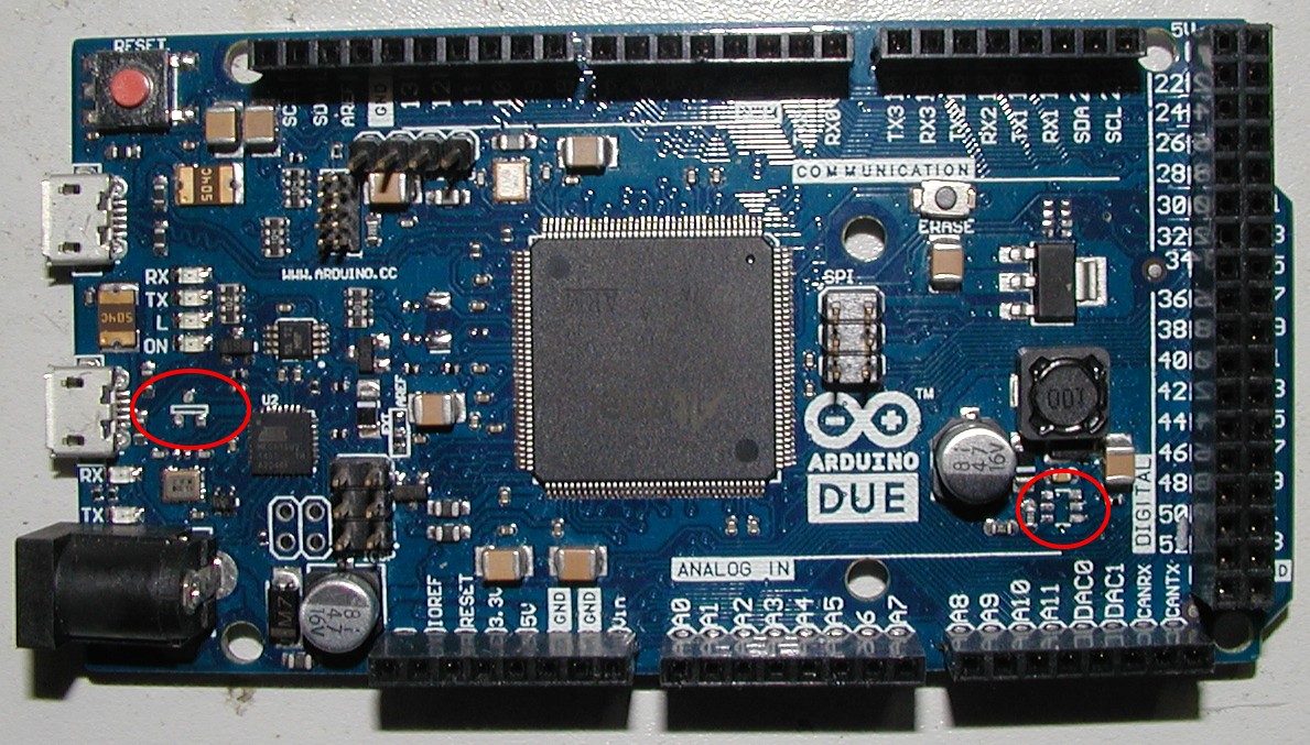
The location of the relevant parts is marked in red in Fig. 2. When hot-air is used for desoldering additional, care should be taken to not affect the 36-pin 0.1" vertical socket (far right). A barrier to the hot air might be sensible.
Hack #5 – Isolate the USB port
Not applicable to module that comes with crowdfunded complete kit
If the previous hack is too radical, there is another possibility that will not only separate USB power lines from the PSU, but also isolate the USB data lines. This makes the PSU completely galvanically isolated from any connected host PC or other USB equipment. That can be accomplished by populating the Auxiliary power module with the following parts:
- USB isolator (IC20)
- Decoupling capacitors C100, C101, C103, C104
- Resistors R120, R121
- Ferrite beads FB6, FB7 and
- A 5-pin header at X10 (or X9 can be moved on that position)
The USB cable that formerly was connected to the Arduino board at X9 must be moved to X10. Removal of the X9 connector makes certain that the USB cabling cannot compromise the electrical isolation of the PSU.
Hack #6 – Communication port protection
Not applicable to module that comes with crowdfunded complete kit
When the previous hack is applied it reduce greatly a chance that due to some fault (hardware, software, wetware) condition the PSU grounding situation will damage connected equipment (e.g. a host PC or logging instrument), and vice versa. But regardless of whether the USB isolation hack is carried out, USB lines can be additionally protected using an ESD protector IC. The same protection can be added to protect Ethernet lines which go to IC26. This can be done by installing the following parts on the Auxiliary power module:
- IC16, C83 for USB, and
- IC15 for Ethernet
Hack #7 – Use of an external W5500 Ethernet module (Obsolete)
This hack is limited to the Arduino Shield r3B4
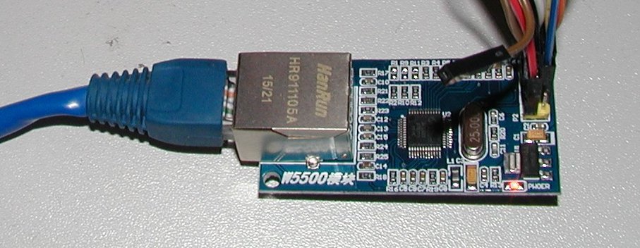
The default means of network communication with the PSU is by using the W5500 Ethernet controller (IC26) located on the Arduino shield. If you are in the process of assembling the PSU and have another widely available Ethernet module, such as one shown on Fig. 3, you can use it temporarily for network connectivity testing even before IC26 and related parts are soldered. To connect this module you’ll require the following:
- Solder 10-pin, 2×5 0.1” header (X20) and
- 10-pin IDC cable
If such a module is planned to be used permanently, take into account that the existing EEZ H24005 model rear panel cannot be used for mounting this module because it’s been punched for an RJ-45 connector mounted on the Auxiliary power module. The X20 pinout is shown in the table below. Please note that it shares the same chip select line as IC26, therefore they cannot both be installed. Neither will operate correctly if so.
|
# |
Pin name |
Description |
|
1 |
+3.3 V |
Not used |
|
2 |
+5 V |
Ethernet module power input |
|
3 |
MISO |
SPI MISO signal |
|
4 |
Gnd |
Ethernet module power return |
|
5 |
MOSI |
SPI MOSI |
|
6 |
RESET |
Reset |
|
7 |
ETH_SELECT |
Chip select |
|
8 |
ETH_IRQ |
Interrupt request |
|
9 |
SCLK |
SPI clock |
|
10 |
n.c. |
Not used |
Hack #8 – Improve high current range precision
Work in progress


