Measurements
Table of contents
- Load transient response testing using MOSFET switch
- Load transient response testing using closed loop load transient tester
- Short circuit recovery
- Capacitive load
- Inductive load
- Output voltage programming (internal)
- Output voltage programming (external)
- Output enable programming
- Change the mode of operation (CV/CC)
- Power on, stand-by and forced power off
- Power on with shorted output
Load transient response testing using MOSFET switch
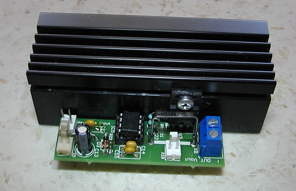
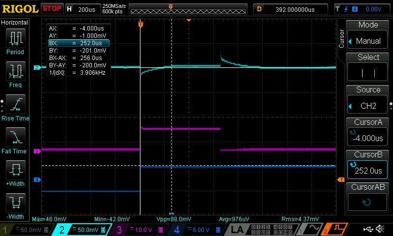
The simplest way to measure load transient response is to use a MOSFET as a fast switch that will connect an additional load in parallel, increasing output current. The MOSFET switch (Fig. 1) is driven with signal generator (blue trace on Fig. 2). Output voltage will be set to 12 V. A permanently connected load of 8.2 Ω, and the MOSFET switch repetitively connecting an additional 33 Ω load will test the transient behavior of the PSU. The output current will alternate between 1.46 A and 1.83 A. The output voltage is shown on the scope image in cyan trace and the voltage on the MOSFET input in magenta. A larger difference between two currents will generate a larger output voltage disturbance; in this case it is -42 mV (or 0.35 % of output voltage) when the additional load is applied (rising edge) and -46 mV (0.38 %) when that load is disconnected (falling edge). The recovery time is marked by two vertical cursor lines and it is about 250 μs.
Load transient response testing using a closed loop load transient tester
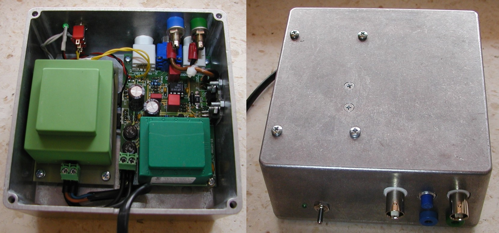
The load transient response could also be tested using the circuit that is presented in LTC’s AN104 application note. The theory of operation is described in detail there. The schematic shown on page 15 (Fig. D1) was built and the resulting PCB circuit installed in a diecast aluminum alloy box (Hammond 1590U) together with two transformers for a bias supply of +/-15 V (Fig. 3). The Eagle, Gerber, files, as well as the BOM for this tester is available on the GitHub.
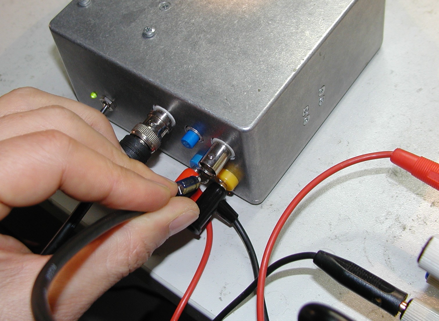
The voltage measurement is AC coupled through home-made probe based on the recommendation the LT application note (pg 14, Fig C1). It used 4.7 μF instead of 10 μF, and at the cable tip an additional 10 μF electrolytic in parallel with a 470 nF ceramic capacitor.
Measurements are conducted on the input terminals of the tester as shown on Fig. 5. The power supply output is set to 20 V with current set to the maximum value to avoid entering CC mode.
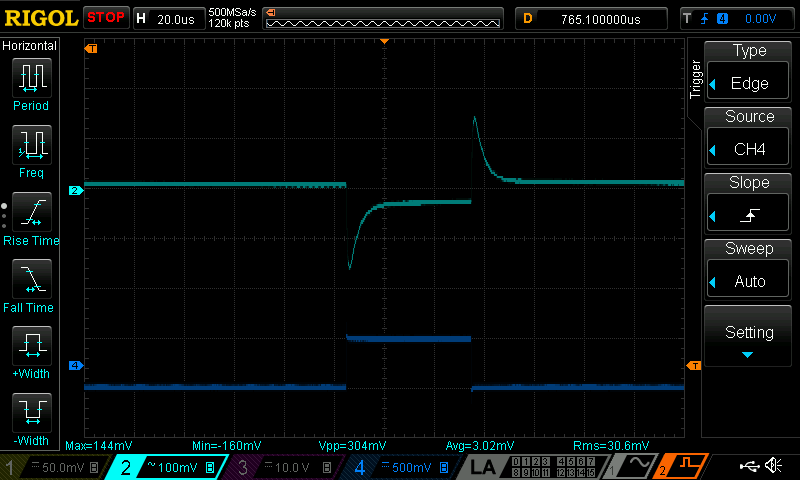
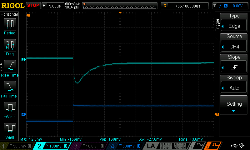
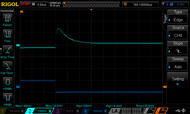
The result is shown on Fig. 6, 7 and 8, and was generated with a 1 Vpp signal (4 kHz, 20 % duty cycle) which corresponds to a 1 A change on top of a continuous load (the DC bias) of 1 A.
Warning: this tester should be used with special precautions if the programmed output voltage of the power supply is higher then 25 V. That could instantly damage the D44H11 switching transistor. The reason is that these conditions exceed the device’s SOA (safe operating area) because it can accept only about 600 mA when Vce is 30 V. Consult the device’s data sheet for more details.
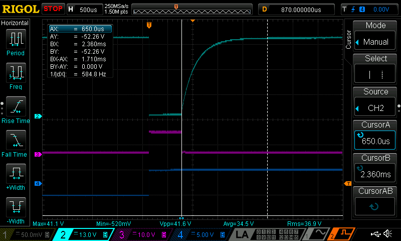
Testing short circuit can be done using the MOSFET switch (Fig. 1) directly connected to the power supply’s output terminals. The output voltage is set to its maximum – for tested model that is 40 V. The output current is also set to a maximum value of 5 A. On Fig. 9, the cyan trace is the output voltage, the magenta trace the MOSFET gate signal derived from the input signal coming from the signal generator (blue trace). Recovery from a shorted output lasts about 1.7 ms.
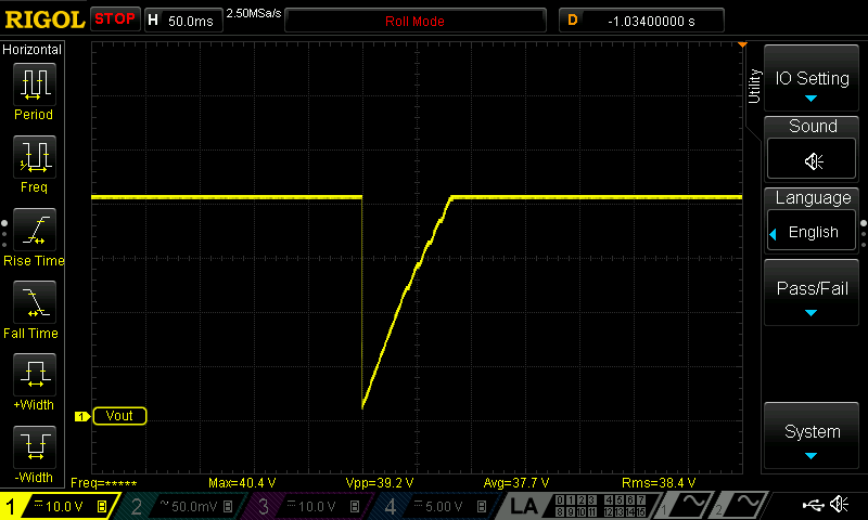
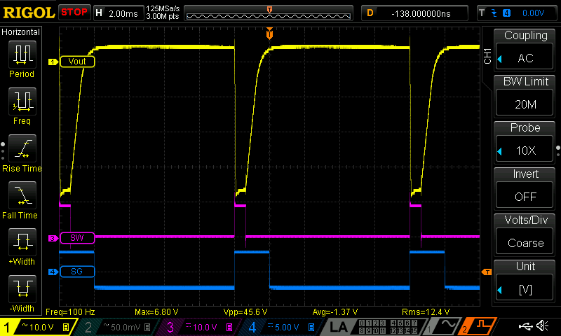
The capacitive load testing is performed by simply connecting a capacitor to the output terminals with oscilloscope probe already connected, A huge output voltage drop is expected from an uncharged capacitor. Fig. 10 shows what happened when the output voltage is set to 40 V and a 10 000 μF electrolytic is connected. Note the capacitor is polarized and must be connected correctly.
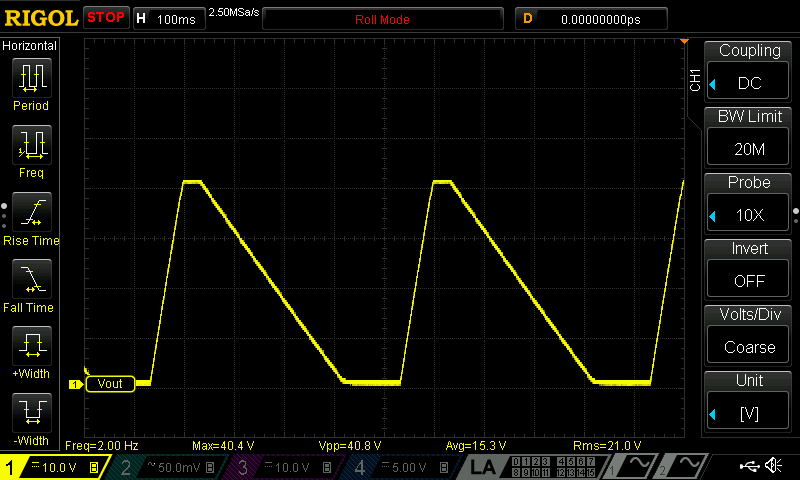
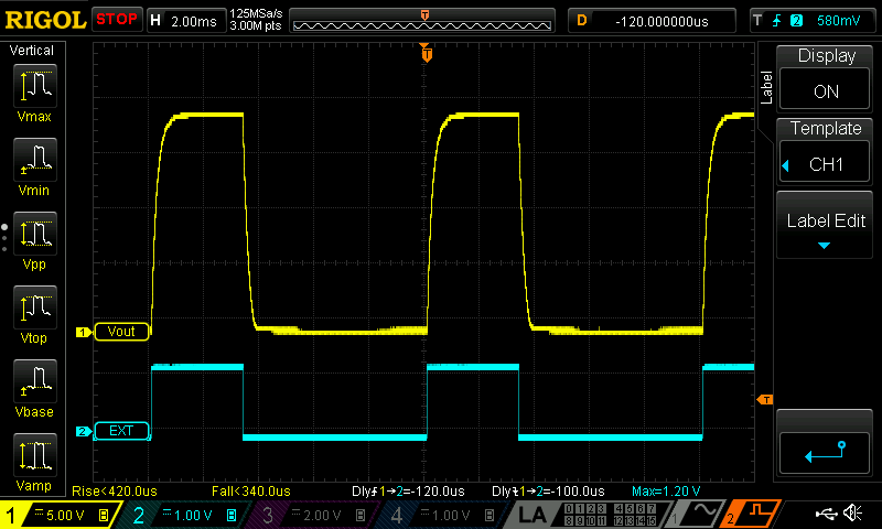
Another scenario was to leave a capacitor connected and program output using the OE signal. The DP (down-programmer) circuit was left active so the charged capacitor can be discharged before the output is enabled again.
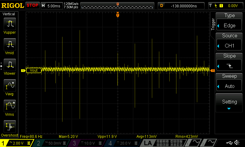
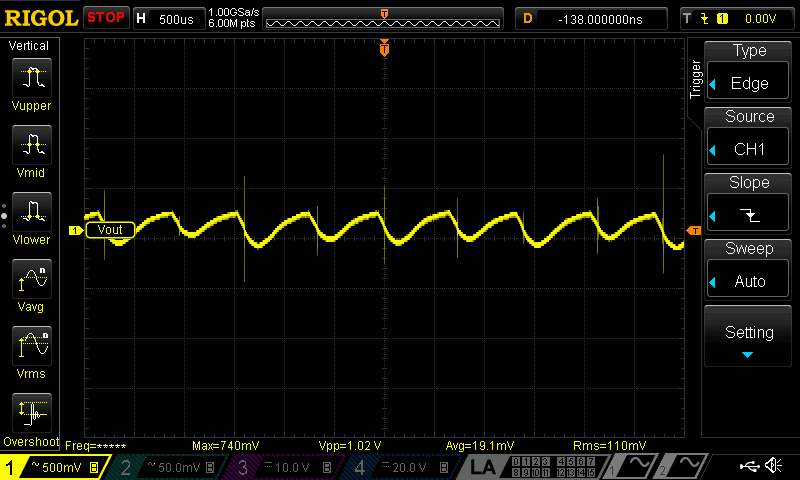
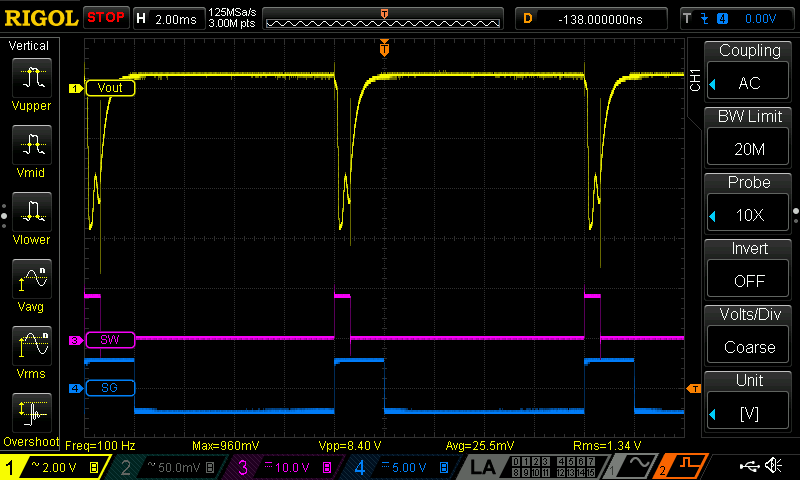
We tested two types of inductive load, a RS540 type DC motor and a 100 μH power inductor (Bourns 2312V series). The DC motor was connected directly and bypassed with additional 100 μF electrolytic capacitor. It generated many spikes, but there was no visible oscillation.
The power inductor was not continuously connected to the output. A MOSFET switcher (Fig. 1), driven with a 100 Hz signal was used (the yellow trace is the output voltage, the magenta is the MOSFET gate signal, and the blue is the signal generator output).
Output voltage programming (internal DAC)
Testing the output voltage programming can demonstrate undesirable overshoots or undershoots when the output voltage is changed from a lower to a higher value, and vice versa. This test also shows the rise (up-programming) and fall (down-programming) times. The result shown in Fig. 16 was generated by changing the output voltage on a 40 V model from 2.5 V (the DAC code is 0x1000) to 10 V (DAC code 0x4000) and back to 2.5 V with no load connected.
Output voltage programming (external)
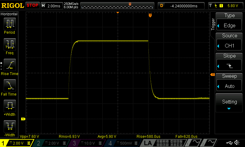
One of the power channel’s voltage outputs can be also programmed from an external source using the protected input accessible via the front panel connector located on the Arduino Shield. As in the case of internal programming, +2.5 V is required for full scale. In this operating mode it is possible to measure the maximum settling time because the input analog control signal is applied directly to the CV control loop.
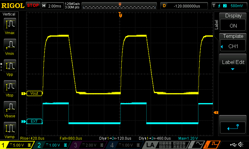
If the programming input is 1.25 V, the output voltage will be set to +20 V (on the tested model) and the difference between the rising edges is the settling time – It is 120 μs as shown in Fig.17 with no load connected. Fig. 18 shows the output with a load connected. External programming can also show the benefit of the down programmer circuit.
With no load, the PSU requires 460 μs to reach zero from half scale.
Change the mode of operation (CV/CC)
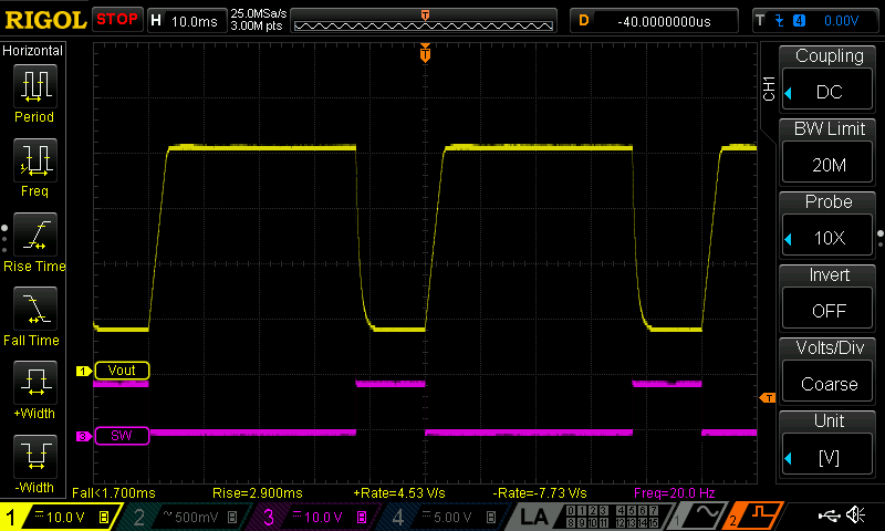
The PSU changes its operational mode when a particular programmed output value is reached. For example, if output current is set to 100 mA, the output voltage (already set to 20 V) will remain unchanged as long as the connected load does not sink more then maximum, current allowed; therefore, its resistance must be equal to or greater than 200 Ω. A sudden change in resistance that could change a mode of operation must be “smooth” – no oscillation nor overshooting are permitted during a transition. This test was performed by repetitively connecting and disconnecting a 33 Ω load with a MOSFET switch (Fig. 1) driven by 10 Hz from the signal generator. The output voltage was set to 40 V (the maximum allowed by the model being tested) and current limited to 250 mA. Therefore when the right load is applied, the PSU should change mode from CV to CC which will cause the output voltage to drop to ~8 V.
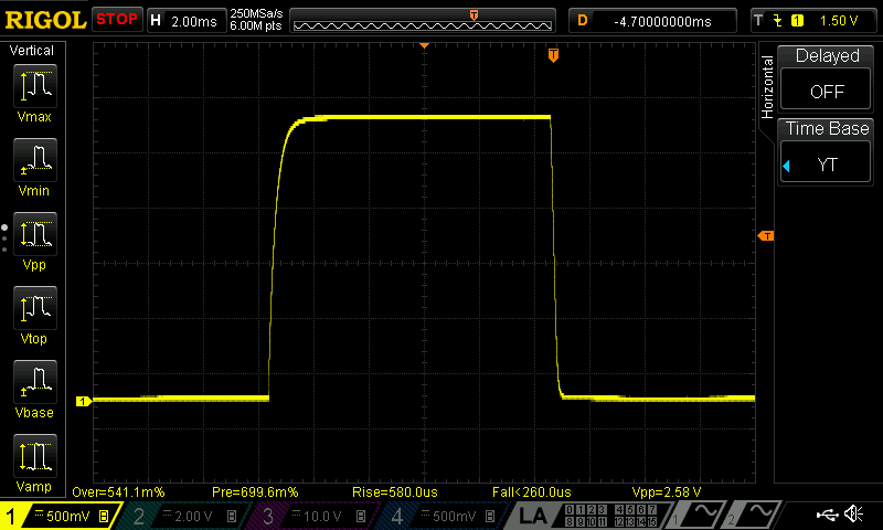
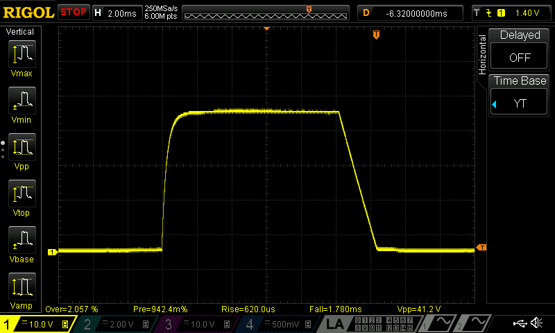
Output enable programming should have the same effect as output voltage programming from a value greater then zero, to zero volts, using the DAC. But since output enable is a different circuit it must be tested separately to test its overshooting and undershooting characteristics. Two cases were tested with no load, changing the output state with the voltage set to 2.5 V (Fig. 20), and then with the voltage set to the maximum (for the tested model) of 40 V (Fig. 21). A difference in fall time (down-programming) is clearly visible (<260 μs versus 1.78 ms).
Power on, stand-by, and forced power off
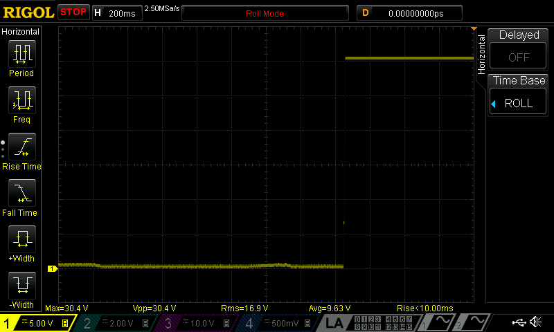
When the power supply is powered on, the output voltage should show no signs of overshoot. In principle, this is the same issue as discussed above – output enable programming followed by output voltage programming. The moment when the power supply channel’s output reaches its programmed value after being powered on is shown on Fig. 22. A well defined transition from no voltage to the set voltage should not be a surprise since powering-on is under control of the MCU firmware, is adjusted long enough after all pre-regulator and post-regulator circuits are stabilized to cause little trouble.
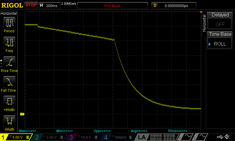
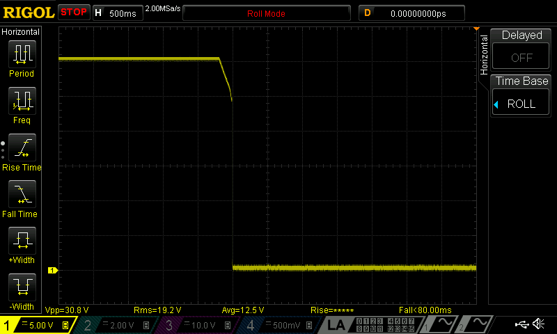
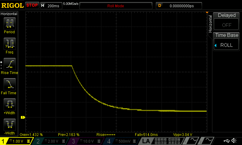
Fig. 23 and 24 show what happens when the AC mains is abruptly unplugged without, and with, a load connected (100 Ω in this case). Therefore no MCU assistance is possible, but no surprises were detected. It’s also true with a very low output voltage set (i.e. below the operational amplifiers bias voltage of 5 V). Fig. 25 shows the state of the output at 3 V and with no load connected.
Fig. 26 shows output when the power off is MCU assisted. It is very similar to entering the standby mode.
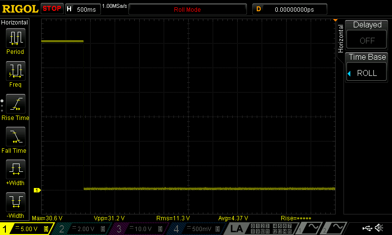
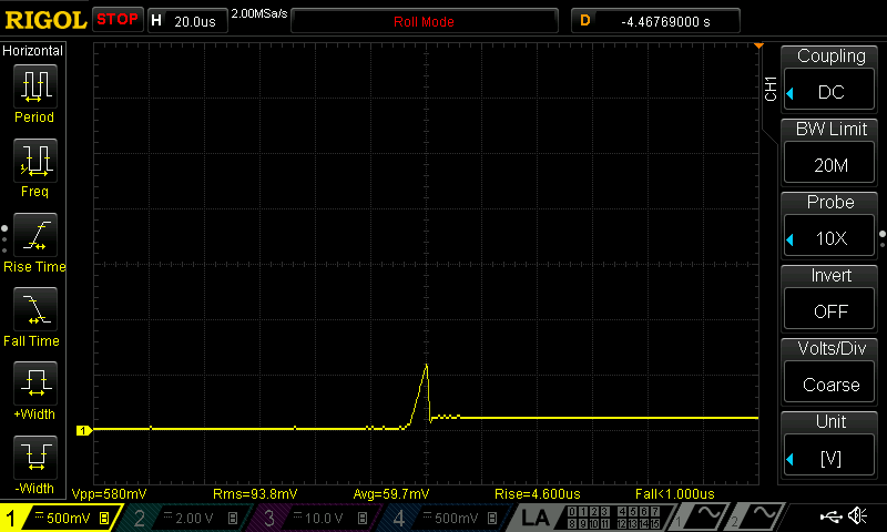
Finally we want to know what will happen at power-up, when both voltage and current are programmed to the maximum level (40 V, 5 A for the model tested here ), and with the output terminals shorted (i.e. with a maximum output demand). Fig. 27 shows the PSU safely enters such mode of operation, and only small peak lasting less then 10 μs can be seen at the output.

