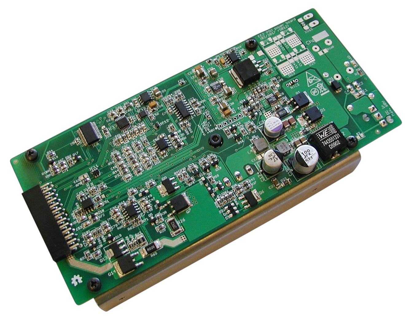
Power board
|
Current version |
r5B13 |
|
Status |
Completed, ready for production |
|
PCB manufactured |
Yes (r5B12) |
|
PCB assembled |
Yes (r5B12) |
|
BOM |
Yes (Farnell, TME, Digikey, Mouser, RS) |
|
File repository |
https://github.com/eez-open/psu-hw/tree/master/Power%20board (include Eagle, Gerber, BOM files and SPICE simulations) |
|
License |
|
|
Contributions |
|
|
Revision history |
2017-09-24: r5B13
2017-03-14: r5B12 (Version 3.0 on GitHub)
2016-12-11: r5B11
2016-10-24: r5B10
2016-07-24: r5B9 (Version 2.0 on GitHub)
2016-06-16: r5B8 – first public release (successor of pre- and post-regulator boards available in Version 1.0 on GitHub)
|
The Power board contains one PSU output channel; two boards are used in the dual channel PSU. This design has at least three distinctive features that make it unusual, or even unique. The first is that the PSU requires a single high voltage input (that can be either DC up to 60 V at the X1 input or AC up to 42 V at the X2 input, see Fig. 2). All required bias voltages are derived from the same source! Therefore no custom made (and costly) transformer (or AC/DC adapter) is required for operation.
Second, it’s a hybrid design and combines the best of two worlds: switching regulation and linear regulation. But the hybrid mode of operation can be changed to linear thanks to the chosen SMPS (Step-Down DC/DC) controller LTC3864. It offers 100% Duty cycle capability which when properly managed with the MCU allows implementing of low ripple mode, described below.
Third, its compact design, and use of only one 26-pin 0.1” header (X3, see Fig. 12) to carry power output and all control lines, simplifies assembly and removes need for several more connecting cables. The only cable remaining is for power input. The Power board is sufficiently self contained as to be portable, and is easily replaceable with another (in case of failure) or new one with a different capability and feature set.
The Power board can be divided into the following sections that will simplify its description and understanding:
- Power input
- Power SMPS pre-regulator
- Bias power supply
- Series/pass element, control loops and dual range current
- Output enable (OE) and Down-programmer (DP)
- Digital control (ADC, DAC and 16-bit I/O expander) and voltage reference
- Voltage programming selection
- CC/CV indications
- Remote sense reverse polarity detection
The Power board capability used in the EEZ H24005 configuration has the following features:
- DC power input (supplied by a Mean Well LRS-150-48 AC/DC module for each channel) which has a maximum output power of 155 W
- Voltage programming: locally (a 16-bit DAC) or remotely/external (+2.5 V for full scale), 0 – 40 V
- Dual range current programming: local (16-bit DAC), 0 – 500 mA, 0 – 5 A
- MCU controlled “Low ripple” mode of operation
For possible modifications and tweaking visit the Hacking area.
The Power board can be connected to either DC and AC input power using the X1 or X2 connector respectively. The AC input option can be used if one has a suitable mains transformer available, or if the proposed AC/DC power module is unsatisfactory. With a properly rated transformer, a maximum output power of 200 W is possible. A potential drawback of using a mains transformer is that its weight will be much more than the AC/DC power modules for the same output power. This will make the PSU much heavier, perhaps impractical if it must be moved frequently from one site to another.
The DC input connector (X1) also has a Protective Earth input connected to capacitors C1 and C2, which are used to reduce differential noise. A common-mode choke, L1, was added to suppress noise appearing on the Power board output if it’s supplied from a switching power supply model as recommended.
The main role of the power pre-regulator circuit is to efficiently decrease input voltage to the output circuits. If only a linear regulator is used (i.e., for post-regulation) there will be enormous power dissipation when outputting a low output voltage; this will be close to the maximum rated power). A large heatsink, combined with a powerful (and noisy) cooling fan will be needed if the PSU is operated this way, even if using only a single channel in an enclosure compact enough to handle and transport easily. For example, if there is a 48 Vdc input to a power board, and we want to deliver 3.3 V, 5 A at the output, the pass MOSFET (Q4) must dissipate over 220 W to deliver only 16.5 W at the output terminals. This is unacceptable.
Switching regulators, by design, do not operate continuously, but alternate between fully on or fully off. By changing their state at high frequency (and filtering out as much of the inevitable high frequency noise as possible) they can output DC voltages more efficiently. The actual efficiency varies depending on the input and on desired output voltages, but 85% and more is easily achievable for high loads (i.e. 1 A and more). This is a considerable improvement over conventional power supplies, and removes the need for very large heat sinks.
If we assume 90% efficiency, with a reasonable switching pre-regulator, and that we require about 2 V difference between its output and the final stage (post-regulator) output (such a margin for a maximum load is enough for good regulation), we will have a quite different thermal situation. In the previous example the pre-regulator was required to decrease 48 V to 5.3 V, while dissipating only 21.35 W ((48-5.3 V) x 5 A x (1-0.90)). Losses in the post-regulator will be only about 10 W (2 V x 5 A). The total is about 31.35 W which will be easily manageable with a medium sized heatsink, or even a smallish heatsink if a more or less small cooling fan is used.
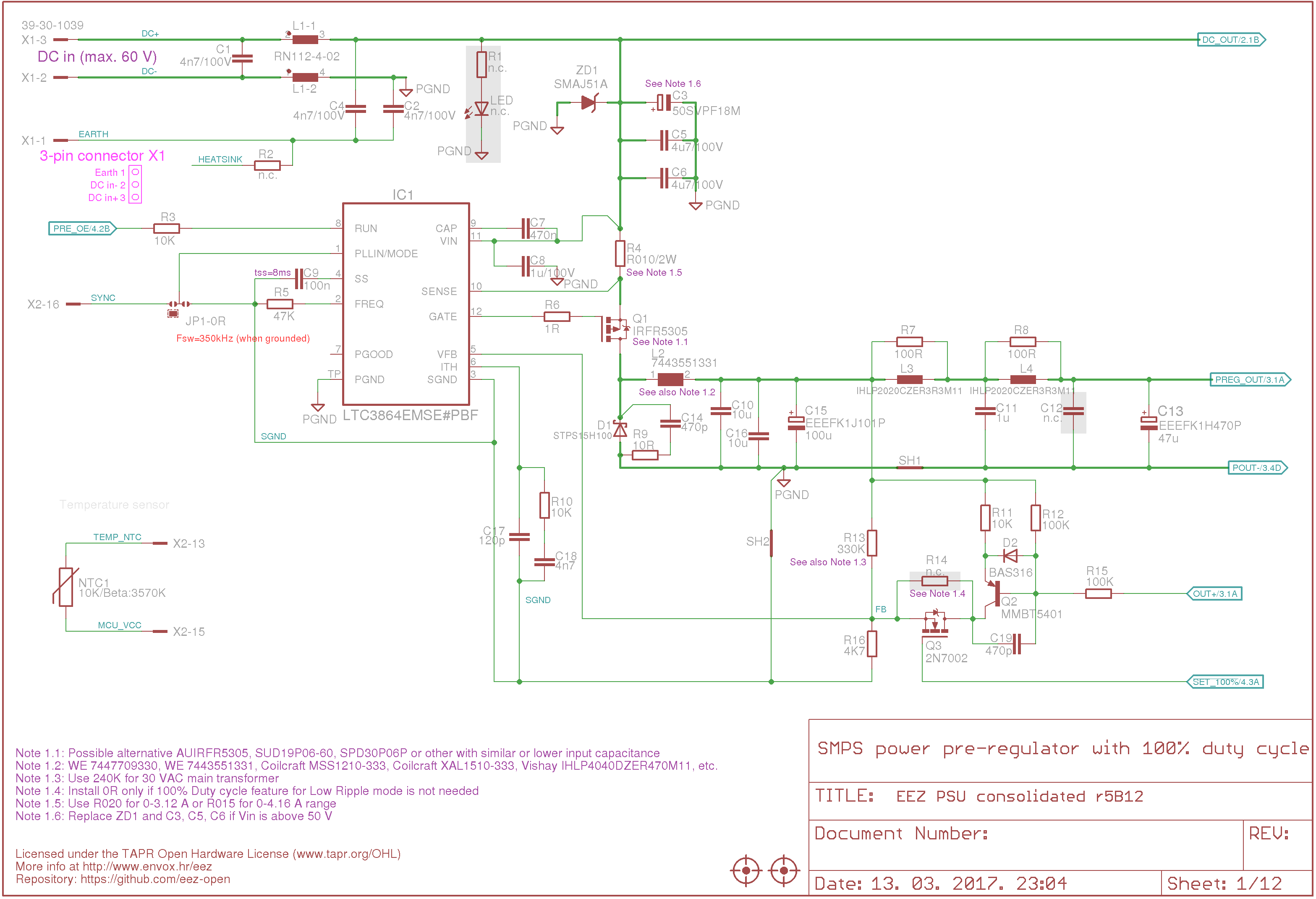
The LTC3864 (IC1) requires a P-channel MOSFET, which is somewhat unusual choice. The required device characteristics are easier to find in an N-channel device (e.g. low Drain-Source on-state resistance (Rds(on)), high current capability, etc.). In general, P-channel MOSFETs are more expensive, but this design requires only one per channel.
The device selected for MOSFET (Q1), is Infineon’s IRFR5305 which has fairly low Drain-Source on-state resistance Rds(on) reducing its dissipation, and also has modest Input capacitance (Ciss), and Total gate charge (Qg), so there is not much load on the LTC3864’s gate driver.
Another crucial component for a switching regulator is its power inductor (L2 in this circuit). We want up to 5 A, and if we want to avoid taking much space on the PCB, we must find an adequate inductor, which was rather challenging. Most commercially available power inductors cannot offer more than 33 μH at a rated (Irms) and saturation current (Isat) of at least 5 A. With an inductor with those specifications, it is in principle possible to maintain the regulator’s operation in CCM (Continuous Conduction Mode), for frequencies below 500 kHz.
The LTC3864 provides current monitoring using current shunt resistor (R2) that provides an output current limit (over-current protection) that will be beneficial in case of short circuit.
Synchronization of switching frequ ency with an external source is done by connecting to the isolated (master) SYNC input at pin 16 (X3). Synchronization helps undesirable sub-harmonic beat frequencies and reduces EMI effects.
If multiple SMPS nodes have a common ground, sync signal isolation will not be required. That is not true in our case – both channels must be isolated to allow serial or parallel connection, increasing the PSU’s flexibility.
The line isolators required to isolate I/O signals for the power module controls are not located on the board itself. They are on the Arduino Shield module and are discussed under Digital isolators.
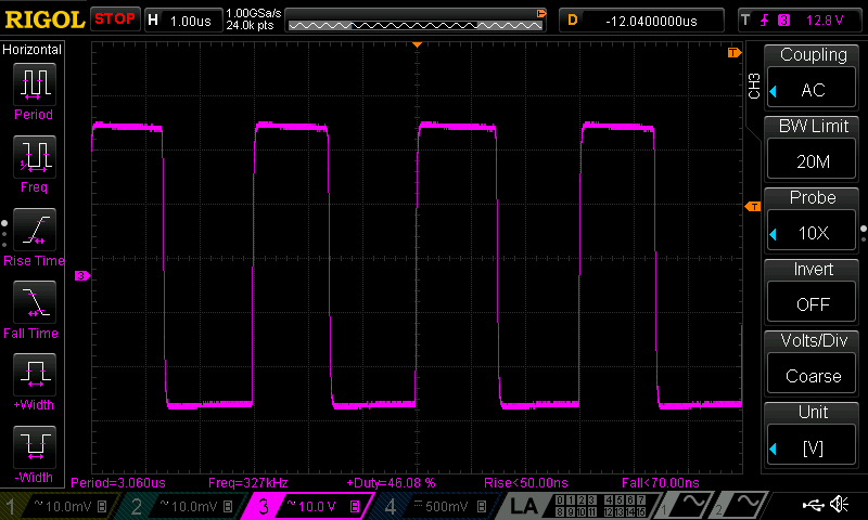
The “free-running” frequency of the LTC3864 (when not using the sync feature) is set via R7 (nominally 47K), and with that value will be slightly less then the master SYNC signal (~300 kHz instead of ~320 kHz) that comes from the Arduino Shield module. A typical switching waveform is shown in Fig. 3 (measured at Q1’s drain with a 1 kΩ resistor).
When channel output is switched off, the LTC3864 (using pin 8) is also put into its micropower shutdown state, drawing only about 7 µA.
Output filtering
The main drawback of any switching regulator is the presence at the output of noise resulting from the high frequency switching operation. It’s often hard to filter out. Low ESR output capacitors will improve the situation to some extent. This PSU does somewhat better still by using additional output filtering (L3, L4, C11, C12, and C13). Of course L3 and L4 must be able to handle at least 5 A continuously for safe operation.
Programming output voltage
The pre-regulator’s operation is interesting. It’s already been noted that a difference of ~2 V is about right to keep the post-regulator’s power dissipation low (about 10W maximum is acceptable). A post-regulator output voltage tracking circuit (Q2) is used to do so.
When a fixed output voltage is required, the output voltage adjustment is done by using the voltage divider (R13, R16) connected between the pre-regulator’s output (but before final filtering with L3, and L4) and the VFB input (pin 5). That voltage level is continuously compared with the internal reference of 0.8 V. The output voltage can be calculated using the following equation:
Vout = 0.8 V x (1 + R13 / R16)
For example, if we want 5 V at its output with R16 set to 4.7 kΩ, then R13 has to be 24.68 kΩ. If R16 is not installed, the feedback loop build around Q2 should provide an appropriate voltage drop to maintain 0.8 V at the VFB input when the post-regulator output is about 2 V below the pre-regulator’s output voltage. If R16 is present, as in our case, it must be high enough to program LTC3864’s output above the input voltage (48 Vdc in our case) to not interfere unacceptably with the tracker circuit (Q2). With 330 kΩ selected, the output voltage will be about 57 V. Another reason it’s set so high is to ensure that, when the “low-ripple” operational mode is chosen, LTC3864 is pushed securely into 100% duty cycle mode.
It’s important to mention that many schematics for a one transistor tracking circuit can be found on the Internet. Most of them may perhaps work well in theory, or in a Spice simulation. But, because all of them – almost without exception – are missing an important part (C19 in the present circuit), they are usually only marginally stable. Without a correctly chosen compensation capacitor, there is likely to be considerable instability under some operational conditions; this may even damage circuit components. The LTC3864 has shown good resilience to such instabilities introduced in the voltage control loop. It gave us enough room to find a workable stability scheme, after some experimentation. We are grateful to Dave Jones of the EEVblog for pointing us in the right direction (Video #329).
Low-ripple mode
Hybrid solutions that combine switching and linear regulators have an advantage when high efficiency and compact design is needed. A switching mode regulator is definitely a better choice if there is a substantial difference between the input and output voltages in the regulator. The main reason for using a linear regulator in the final stage is a better dynamic response (i.e. to load transients) and better stability over a wider range of output voltages and currents. There is also an additional noise attenuation effect from a linear regulator final stage. But such designs can be tricky. Even with an excellent linear regulation final stage, a less than ideal PCB layout will defeat the noise filtering effect, and could even introduce instabilities. Using only a two layer PCB instead of multiple layers (4 or more) PCB might not allow good enough performance. We chose a two layer PCB, largely because of the lower cost.
Measuring output ripple and noise is thought by many to be a black art. It seems that many manufacturers publish only results that look better than the competition, without spending much time on less than spectacular specification and performance details. Even special measurement techniques (e.g., using additional capacitors at the output, in parallel with the load, favorable choices in output voltages and currents reported, etc.). Generally speaking, only a measuring bandwidth of 20 MHz is mentioned.
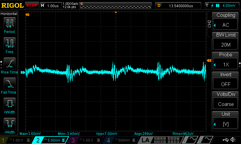
The measurements taken for this PSU, and the methods used to acquire them, are reported in Measurements. Those values are more than merely adequate, and compare favorably with high quality, and much more expensive, commercial units. The same is true for output ripple and noise. An example of the standard PSU’s ripple and noise with a 16.4 Ω load is given in Fig. 4.
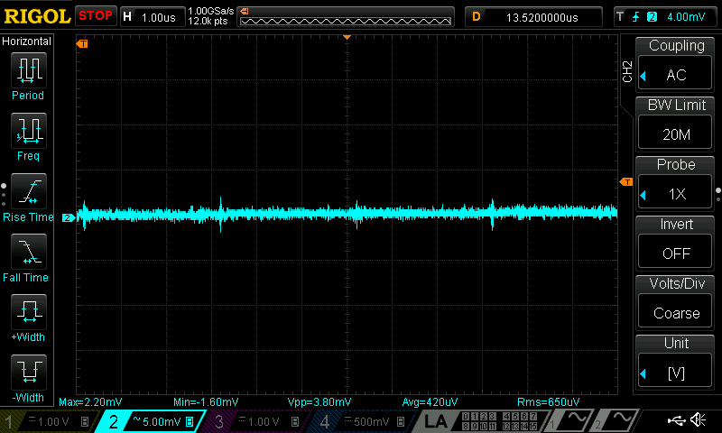
Thanks to the LTC3864’s performance, working in the low ripple mode, it’s possible to reduce output ripple and noise figures still further at the expense of voltage and current capacity. For example, with the same load connected as above, but with the output voltage decreased to 0.5 V, the PSU will enter low ripple mode of operation, cutting noise and ripple in half (Fig. 5).
The low ripple mode of operation must be managed by the MCU to limit maximum power dissipation of Q4. It is possible to change the maximum power dissipation limit in firmware, but it should not exceed 30 W for low ripple (Q1 operating in saturation). The worst case, dual channel operation, is 60 W. This is established in part by the thermal cooling capacity in the enclosure.
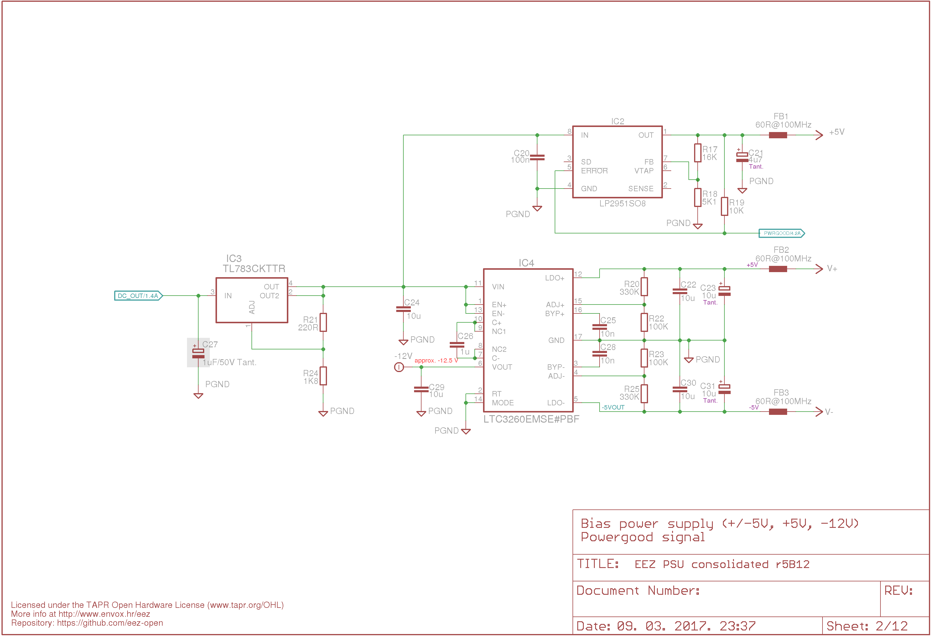
The bias power supply (Fig. 6) has two stages: a high voltage LDO (IC3) and low voltage LDO’s for final regulation. The high voltage LDO was selected because the total required bias power is small; the TL783 (IC3) used comes in a D2PAK package which can easily dissipate about 1.5 W when decreasing 48 V down to about 12 V.
LTC3260 (IC4), an inverting charge pump, is used to provide symmetrical low noise regulated outputs of +5 V and -5 V for the linear circuits. It has also the negative voltage output (VOUT, at pin 6) required for reliable down-programmer (see below) activation.
The digital section has its own power rail provided by an LP2951 which was selected in part because of its “Power good” indication (ERROR output at pin 5) which can be used for checking a power line’s “health”. The MCU will not enable power output during start up until that signal is low. Also, if this signal becomes low during normal operation, the firmware will execute a routine which forces the PSU into standby mode.
Series/pass element and control loops
The analog section of the post-regulator stage in this design was inspired by the exceptional work of Leonid Ivanovitch which was published on the EEVblog forum.
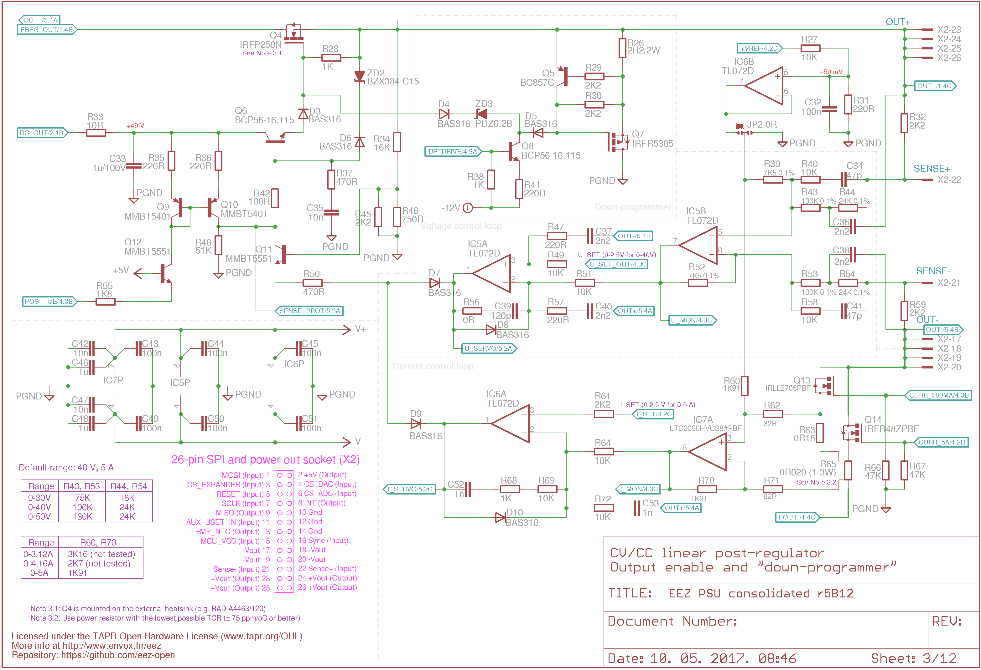
An N-channel MOSFET (Q4), connected as common drain, is the series regulator. It operates continuously in linear mode when the channel is enabled. Therefore, its SOA is the key design criterion, and has been carefully considered during design and component selection. Thermal design is very important and MOSFETs with low ZthJC (junction-to -case transient thermal impedance) are the most suitable.
Q4 requires a bias voltage for normal operation; this is applied on the MOSFET’s gate so that it is a few volts above the drain voltage. Commonly for that purpose an additional bias power source derived from an auxiliary secondary transformer winding, or a charge pump is needed. The output of this source floats on top of the drain voltage since its negative output is connected there, ensuring a constant difference between the gate and drain voltages regardless of the input voltage at the drain. Instead of a dedicated gate bias supply, this PSU design uses input voltage. The input voltage has to be 5 V or more above the maximum output voltage. That requirement is met with Vin at 48 V in the PSU’s 0 – 40 V range.
The zener diode ZD2 ensures the gate-source voltage (Vgs) stays within allowed limits (i.e. below 13 V).
Diode D3 protects Q6 from base-emitter junction breakdown, and D4 (as with D6) was added to prevent current flowing from any external source if the output has been switched off.
The output voltage on Q4 is controlled by two control loops: constant voltage (by IC5), and constant current (by using IC6 and IC7). In general, only one can be active at a time. Diodes D7 and D9 ensure that the output signal from one of the control loops does not affect the other loop. Q11 is a common base voltage amplifier stage and R34, R45, R46 control local negative feedback.
Both control loops use the same precision voltage reference (IC9, Fig. 12) in supervising output voltage and current. The voltage reference is +2.5 V. Therefore, the gain in both control loops must be adjusted so the output range returns a positive value between zero and +2.5 V. That is done by selecting the feedback loop resistors for IC5B and IC7A which are connected as differential amplifiers. For example, if we’d like to have the output voltage in the range from zero to 40 V, IC5B’s gain must be 2.5 / 40 = 0.0625 (in effect, the output signal measurement must be attenuated by a factor of 16).
In practice, due to component tolerances, it is likely the highest values (e.g. 40 V) will not be reached, and a few tens of mV below maximum voltage will be the actual limit when the maximum DAC voltage (generated by the 0xFFFF code) is applied to the non-inverting input of IC5A.
The same problem can be expected on the other end of the voltage range; the minimum DAC voltage (generated by the 0x0000 code) will not get the output voltage down to zero, but to only a few tens of mV above zero. This issue is more important, because it requires a negative DAC voltage – not possible with the DAC chip used (IC10, Fig. 12) without adding an additional operational amplifier. Fortunately such “shrinking of range” can be easily overridden with two simple changes:
- at the high end, we need to change the gain factor, and
- at the low end, move the reference ground potential from zero to, say, 50 mV (applied on IC5B and IC7A non-inverting inputs)
The voltage loop gain (for IC5B) can be set to, say, 0.060484 with a combination of 7.5 kΩ (for R39, R52) and 124 kΩ (for R43+R44, R53+R54). For the current loop (IC7A), we can change the gain from an “ideal” of 25 (i.e., 5 A across a 20 mΩ sense resistor gives 100 mV and 2.5 V / 0.1 V = 25) to, say, 24.39. A combination of 2 kΩ (R60, R70) and 82 Ω (R62, R71) does this.
A new reference ground potential of about 50 mV can be derived from a +2.5 V reference (IC10) by using the voltage divider R27, R31, and buffering it via IC6B. The offset on the lower programmed output value must be taken into account in firmware, however.
Output voltage can be “sensed” locally or remotely. In the first case the inputs at X3-22, and X3-21 must be connected to the power output pins (X3-23…26, X3-17…20). In the second case, the connection is done via the load’s input terminals using a separate cable (i.e. Kelvin wiring) connected directly to the load’s terminals. The PSU firmware manages this through the signal relay (K_S1, K_S2) located on the Arduino shield. The remote sensing cable can be shielded, but the cable shield must be connected to an earth protective terminal only on one end to avoid ground loop problems.
Current sensing and ranges
The output current is measured by the voltage drop across a current sense resistor (R63 or R65), and the current range can be also set by changing the values of those resistors – higher values will produce a higher voltage drop for the same current, and therefore IC7A’s gain will be reduced. We can improve the precision of the measured value, but using too high a value could produce excessive heating in the current sense resistor. The dissipated power will rise with the square of the current, and the heating will cause changes in the value of the resistors.
It is important to take into account any heating of the current sense resistor, since it decreases accuracy because its resistance is temperature dependent. Choosing a resistor with a low TCR even while keeping dissipation low will be best. Using the 20 mΩ value chosen and a maximum current of 5 A, the dissipated power will be 500 mW. The resistor chosen for R65 has a TCR of 75 ppm/oC temperature; at maximum current for this PSU design a resistance change of up to -0.36% can be measured.
Output current is limited and measured within two ranges: LOW (500 mA) and HIGH (5 A). Selecting the current range is done by switching between two current sense resistors (R63 or R65) using MOSFETs Q13 and Q14. The HIGH range MOSFET, Q14, should have an Rds(on) as low as possible to reduce the heating which might affect measurement precision regardless of the current sense resistor temperature stability (TCR).
Since voltage and current are programmed separately, any combination of output current and voltage is possible. This means that a dual channel asymmetric power supply could be built with different Power board capabilities (e.g., two different output ranges such as 0 – 40 V / 5 A and 0 – 30 V / 3.12 A, and so on).
Output enable (OE) and down-programmer (DP)
The PSU’s Output enable control is a two-state circuit which allows emergency shut down if necessary (e.g. the connected load is overheating, perhaps because of erroneously programmed voltage and current levels). The output enable circuit consists of a Q9, Q10 current mirror controlled by Q12 and Q16 (Fig. 12) that regulates the bias voltage at Q4 delivered by Q6.
The down-programmer (DP) circuit is built using Q7, Q5 controlled by Q8 and Q15 (Fig. 12). It’s used to improve output voltage fall times (hence the name, down-programmer).
Fall times (from a previously programmed higher voltage output to a lower voltage) will be up to an order of magnitude smaller because of this provision. PSUs without such provisions may delay reduction in output voltage because of energy (ie, charge) stored in the PSU’s output capacitor; it could actively supply power to a load for some time. As well, capacitance in the loaded device might do the same.
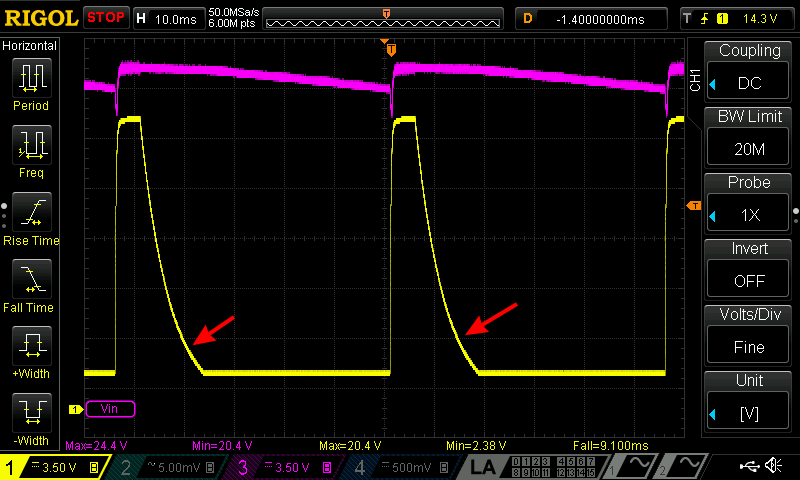
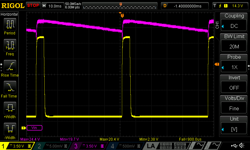
The difference in programmed output (yellow trace) depending on the DP state is shown below. The PSU’s output has been programmed with steps from 20 to 1.5 V (10 ms on, 50 ms off) and a 450 Ω load. Fig. 8 shows output without, and Fig. 9 with DP circuit activated.
When used, the common practice for any down-programmer circuit is to follow the state of the output enable circuit; it is enabled when output is enabled, and vice versa. The down-programmer circuit on the Power board could be controlled independently if required. Its default state is on, therefore the DP control circuit will be disabled when 5 V is applied to its input (DP_DRIVE signal).
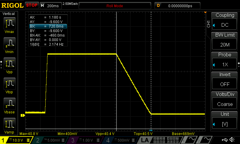
Of course, the down-programmer has a finite current sinking capability (limited to about 300 mA via R31). This can be seen when a load with a large capacitance (or just a capacitor) is connected to the output. Fig. 10 shows this PSU’s fall time of 460 ms with 3 300 μF capacitors charged to 40 V.
Digital control (ADC, DAC and the 8-bit I/O expander); and the voltage reference
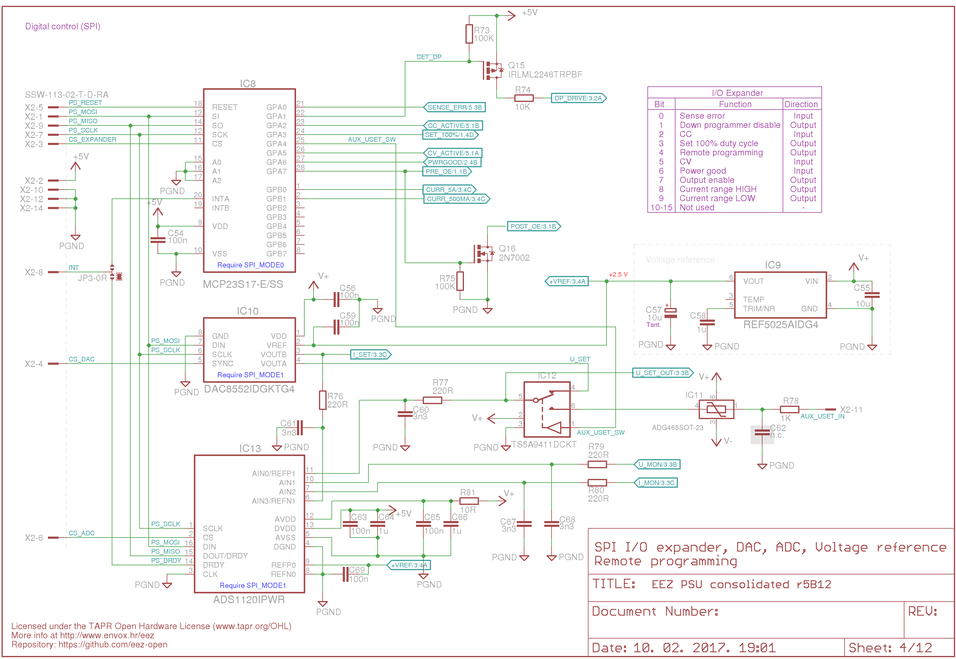
The post-regulator is an analog circuit controlled by analog control loops. Any control function done digitally (e.g., via MCU firmware) requires signal conversion. Three devices are added to support this requirement (see Fig. 12):
- DAC8552, a dual channel 16-bit Digital to Analog Converter (IC10),
- ADS1120, a 15-bit delta-sigma (ΔΣ) Analog to Digital Converter (IC13), and
- MCP23S17, a 16-bit I/O expander (IC8)
IMPORTANT: All digital devices are powered by 5 V, therefore they cannot be directly connected to the Arduino Due (or to any other 3.3 V MCU board). Also if more then one Power board is to be connected to a single MCU board, their SPI buses must be isolated from each other even if the MCU board used is capable of working with 5 V logic levels.
Digital to analog converter (DAC)
The DAC is used to control the voltage and current for the power supply. Using a SPI bus, the MCU communicates with the DAC to program a new voltage at the DAC’s outputs (U_SET and I_SET). This chip also includes a power-on reset circuit which ensures that the DAC outputs power up at zero, and remains there until an explicit command from the MCU firmware takes place.
The range of voltage the DAC can manage is determined by the voltage at its reference pin (Vref) which is connected to the precision voltage reference of +2.5 V (IC9).
An important parameter determining the DAC speed (and so the response time PSU) is settling time which is the elapsed time from input code write (i.e. a command from the MCU) until the output arrives at, and remains within, the specified output value. More precisely to a value within the permitted error band around the final value. For this PSU design, this is at most 10 μs. Another issue is the delay in issuing a command to the DAC. For this device, commands are written to the DAC by sending 24-bits (the first byte is the command/register selection, and the remaining two bytes (i.e. 16-bits) are converted into an analog voltage). The SPI clock frequency used for transferring 24-bit value can be as hight as 30 MHz (!). The DAC’s performance specification provides enough margin to use it efficiently for PSU programming where new output values change in milliseconds (even including the execution time of the necessary MCU code).
Analog to digital converter (ADC)
The ADC is equipped with a four channel input multiplexer, and can manage up to 2 000 samples per second. Its SPI clock is 4.096 MHz (4.5 MHz max). It’s used to measure voltage and current control loops levels (U_MON, I_MON), but also the DAC outputs (U_SET, I_SET). The ADC used is a 16-bit bipolar device which gives 15-bit resolution (positive half) of the full scale (the negative half is not fully used; it monitors down-programmer sinking). It also comes with an internal +2.048 V voltage reference. The ADC’s other features aren’t used in this PSU design at present.
In contrast to the DAC, the ADC requires bidirectional communication with the MCU. The ADC’s output transfers results of data acquisition at the end of each measurement. The DOUT/DRDY output is connected to the MISO line to do this. That output could be also used to notify the SPI master (MCU) that the data acquisition cycle on the selected input (one of four) is done and that data is ready to be read from the ADC. Another possible arrangement is to use the dedicated DRDY output as a notification to the MCU. The JP3 jumper uses the DRDY signal to force an MCU interrupt, though, of course, a polling routine could be used to periodically acquire converted data.
16-bit I/O expander
An I/O expander is installed to minimize the number of signal lines needed between a Power board and the digital controller (via the Arduino Shield). The expander’s I/O lines are used as follows:
|
# |
Direction |
I/O name |
Active |
Description |
|
0 |
Input |
SENSE_ERR |
Low |
Reverse remote sense polarity detected |
|
1 |
Output |
SET_DP |
Low |
Enable (or disable) the down programmer circuit |
|
2 |
Input |
CC_ACTIVE |
High |
CC (constant current) mode of operation is active |
|
3 |
Input |
EXT_PROG |
High |
Remote output voltage programming source selection |
|
4 |
Output |
SET_100% |
Low |
100% duty cycle mode control |
|
5 |
Input |
CV_ACTIVE |
High |
CV (constant voltage) mode of operation is active |
|
6 |
Input |
PWRGOOD |
High |
Power good input has been received from the pre-regulator module |
|
7 |
Output |
SET_OE |
High |
Enable or disable power output |
|
8 |
Output |
CURR_5A |
High |
Set the high current range resistor |
|
9 |
Output |
CURR_500MA |
High |
Set the low current range resistor |
|
10-15 |
– |
– |
– |
Not used |
Resolution
One of the starting requirements for this project was a resolution of 10 mV and 10 mA, and an output range of up to 50 V and up to 5 A. Those requirements require that the resolution of the digital devices used in programming and monitoring output voltage and current be 5 000 programming steps (for a 50 V range). Therefore DAC and ADC resolution must be 13-bits or higher to provide 8 192 or more values (e.g. 12-bits gives as only 4 096 possible combinations, and so doesn’t meet the requirement).
The DAC and ADC devices selected meet several criteria: interface connections, speed, availability (i.e. no exotic sources) and, of course, cost. The devices chosen for the post-regulator provide decent price/performance in a PSU design, giving 16-bit programming resolution and 15-bit measuring resolution. Theoretically, the following precisions could be achieved:
|
Range |
16-bit programming |
15-bit measurement |
|
0 – 30 V |
0.457 mV |
0.916 mV |
|
0 – 40 V |
0.610 mV |
1.22 mV |
|
0 – 50 V |
0.763 mV |
1.53 mV |
|
0 – 3.12 A |
0.0476 mA |
0.0952 mA |
|
0 – 4.16 A |
0.0636 mA |
0.127 mA |
|
HIGH: 0 – 5 A |
0.0763 mA |
0.153 mA |
|
LOW: 0 – 500 mA |
7.63 μA |
15.3 μA |
For the EEZ H24005 model, it is realistic to expect 10 mV output voltage programming and measurement resolution, and a 1 mA (HIGH range), or well below 0.1 mA (LOW range), output current resolution.
Output voltage programming has already been covered in the reference voltage discussion for the CV control loop. The digital programming is managed by the MCU, so a user can remotely set desired voltage level using SCPI commands to the firmware via the USB or Ethernet interfaces, or locally via the TFT touch-screen display attached to the Arduino Shield.
Additionally, voltage programming can be performed by supplying a positive analog signal (+2.5 V for the full scale). The Arduino Shield has a terminal near the channel output binding posts (X12, X14) reserved for just such remote analog programming. Only one reference signal can be used at a time which is managed with an analog multiplexer/switch (IC12). The default setting is internal. Analog programming is faster, but additional care must be taken to stay within the safe working range even though there are protective circuits (IC12 and the TVS diodes ZD7, ZD10 on the Arduino Shield). Since the MCU can monitor the U_SET signal even when analog voltage programming is used, it’s possible to implement at least an over-voltage protection (OVP) that will switch channel output off if the applied control input signal will cause an unacceptable output voltage.
One of the uses for the analog programming feature is to use the PSU as a tracking pre-regulator, perhaps while experimenting with another adjustable linear power supply. In that case, we would like to keep dissipated power within safe limits because a suitable heatsink might be missing in an experimental phase, or some other flaw in design or testing might cause dangerous heating. Another reason is to test how well a power supply under test works at some chosen difference between input and output voltages.
When its output is enabled, the PSU can work in one of the following operational modes:
- CV (constant voltage): the voltage control loop circuit (around IC5) is setting the output voltage. This mode is the default for power supplies with series regulator elements.
- CC (constant current): the current control loop (IC6, IC7) is setting output voltages, and thereby limiting output current, and
- UR (unregulated, i.e. not regulated): neither the output voltage nor output current are controlling the PSU’s output.
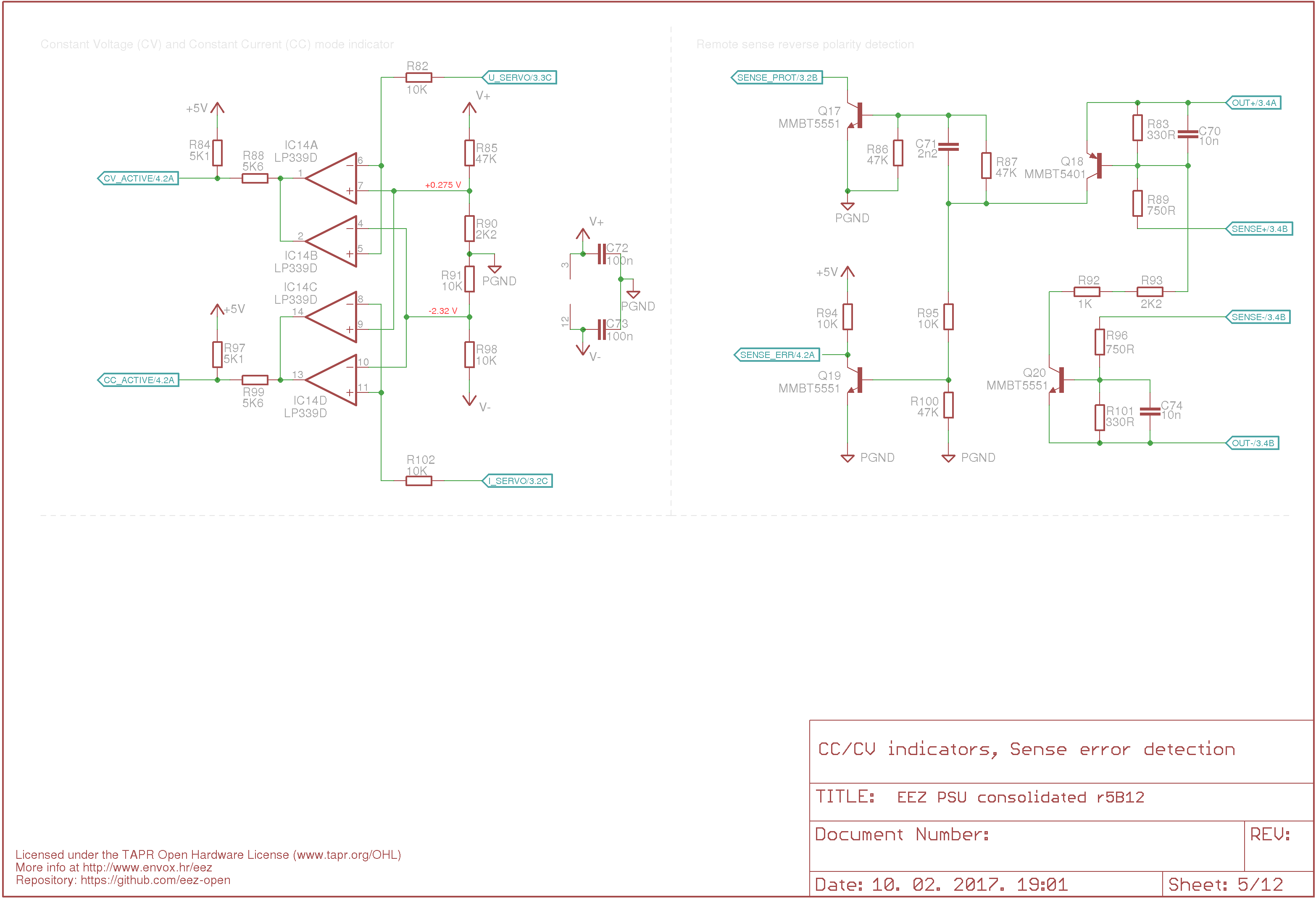
The CC and CV circuits use “window comparators” that require two comparators: one detecting lower and one the upper levels. The CV signal is generated by comparing the U_SERVO output from IC5A using IC14A and IC14B as the window comparators. In the same fashion, the CC signal uses the I_SERVO output from IC6A using the IC14C, IC14D comparators. The signals produced are level shifted for TTL inputs (using the R86, R89 and R98, R100 voltage dividers).
Remote sense reverse polarity detection
Remote voltage sensing is necessary to insure precise output voltage programming regardless of output current. It is essentially impossible to deliver power to a load with 1 mV precision without remotely sensing the voltage at the load’s input terminal, perhaps at the end of a cable a meter or three away from the PSU’s output terminals. Output currents of a few amperes through insufficiently robust connection cables, or to load terminals with a resistance in miliohms, could easily produce a voltage drop across the cable from a few milivolts to even a few hundred milivolts. When using remote sensing, the output voltage actually supplied to the load is not measured at the PSU outputs but at the connected load terminals. The CV control loop (i.e. the error amplifier and correction circuitry) can compare that voltage against the programmed one, and all the voltage drops along the cable will have no effect. The technique is generally referred to as “Kelvin sensing”, or 4-wire measurement technique.
Exposing the voltage sensing inputs to some external connection has disadvantages, however. The major one, not always obviously so, is that any or both of the sense cables can be mistakenly connected in a reverse polarity fashion. This is likely to cause troubles. Internally, local sensing will be correct because the signal relay on the Arduino Shield board will insure the correct connection to the voltage control circuitry (i.e. Sense+ to Out+, and Sense– to Out–).
When remote inputs are disconnected from the load input power connectors (via mistake, someone tripping over a cable, failure of an alligator clip to live up to its namesake’s grip, or just the perversity of things,…), the PSU can still work safely because they will still be properly polarized thanks to R32, R59. There will be only a small deviation in output voltage because of the addition of 2 x 2 kΩ to the input voltage divider of IC5B.
If a sense wire is connected to the opposite polarity power output, there will be a serious fault condition for the input signal will have no relation to the channel attempting to ensure correct voltage and current to the load. There will be a maximum error bias within the CV control loop; it will try to compensate, and the end result will be the maximum possible voltage on the output. As one may imagine, this could easily result in irreparable damage to the connected load.
To avoid some of these unfortunate events, a reverse polarity detection circuit (Q18, Q20) has been added in parallel with the remote sensing inputs. It has two purposes: first, to immediately decrease output voltage to under approx. 1.7 V (Q17), and to generate a SENSE_ERR signal (Q19) that will notify MCU to immediately disable output.
Regardless, it’s still a very good practice to limit output current supplied to a load to only a small current above that expected by the load device when it’s in normal operation. If there is no understanding of what the circuit should normally draw, it’s time for more thought and analysis of the circuit, not time to power it up. The magic smoke might get out.
PCB layout
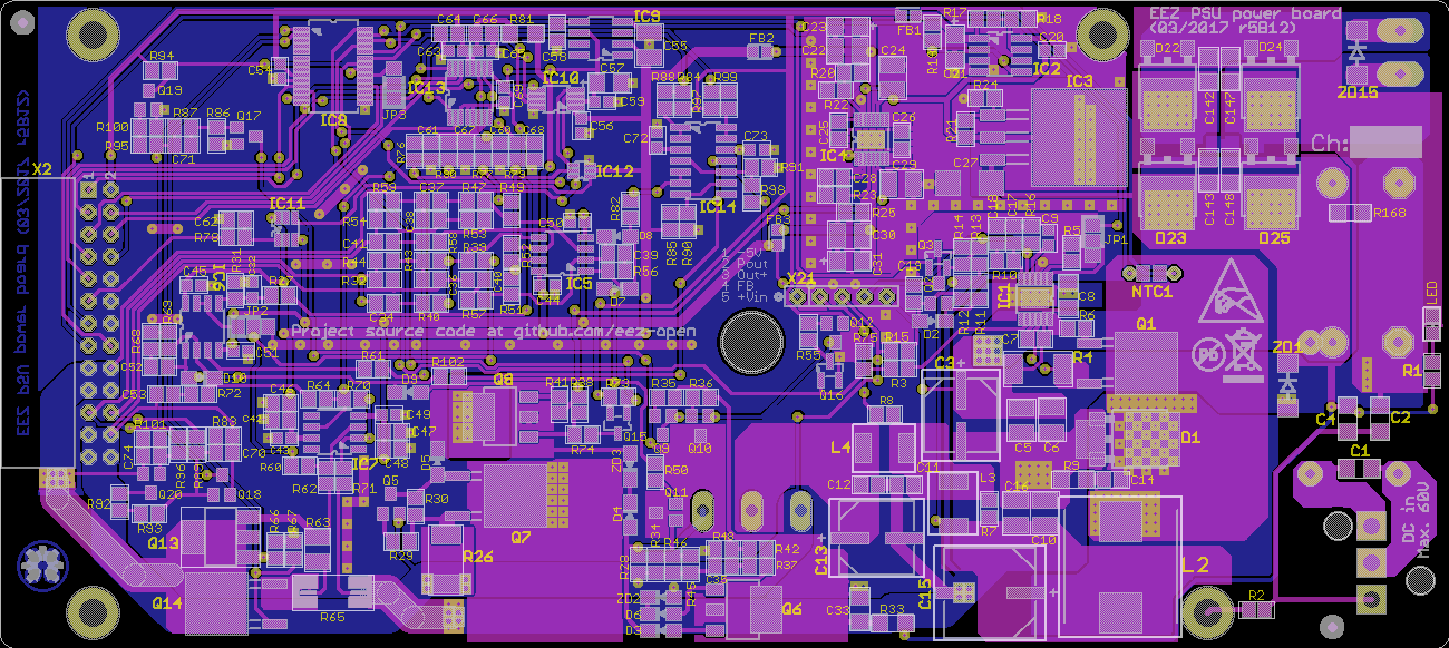
The PCB layout shown in Fig. 13 includes all the mandatory and optional parts from the circuits discussed. Both DC and AC power inputs options are supported. The two layer PCB (laid out with Eagle, but without the autorouter) puts many limitations on arranging this fairly complex design in such a limited space. One goal was to house everything in an enclosure no taller then the 2U (89 mm) form factor. Another limitation is to provide sufficient cooling for the power SMD components (i.e. Q1, D1, L2, but also IC1, Q5, Q14, R65) and the main THT power component (Q4).
The vertical orientation of the two Power board PCBs facing each other was chosen to create a kind of flow tunnel when the top and bottom enclosure plates are installed – this is the intended operational condition and the PSU should not operated without them. The ∅60 mm cooling fan should be located on the one end of the tunnel structure, while on the opposite end both Power boards are connected to the Arduino shield. Both top and bottom enclosure plates require multiple ventilation slots to ensure good air flow, and to cope with the possibility that either top or bottom holes might be blocked in some way. Common possibilities include manuals, data sheets, or anything else from a cluttered work bench. There are feet provided for on the bottom plate which should provide airflow through the bottom plate slots even when the top panel slots are blocked.
The height of the Power PCB is 74 mm which fits within an 80 mm enclosure. They are screwed to an U-profile heatsink (custom made by Varisom) which is fixed to the enclosure’s top and bottom plates.
The PCB’s top side is oriented toward the tunnel interior to maximize air flow over the SMD components. Due to their size some THT components: X1, L1 (DC input) and X19, C144, C146 (AC input) are mounted on the bottom side of the PCB.
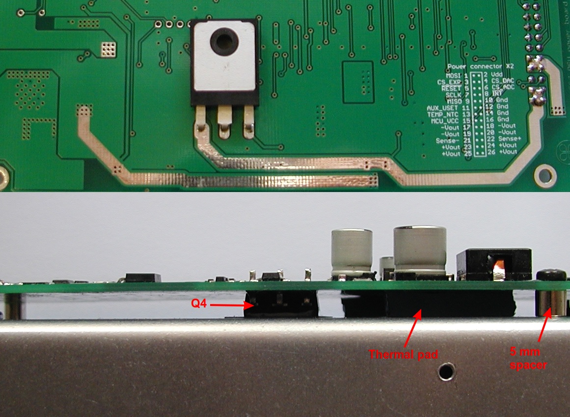
Q4 (Fig. 14) and its heatsink are also mounted on the bottom side. Four 3.2 mm holes are provided to mount the PCB to the heatsink using 5 mm spacers. Additionally, cooling of critical SMD components (i.e. Q1, D1, L2, and IC3) can be further improved by putting a “thermal bridge” between the bottom side of the PCB and the Q4 heatsink. A 5 mm thick conductive silicone thermal pad is highly recommended.
The PCB layout uses a single ground plane that occupies most of the bottom side. Components belonging to the power pre-regulator, bias pre-regulator, and analog and digital circuits are strategically grouped together, and separated from other circuitry to decrease interference. This Power board is a great candidate for a 4-layer PCB which could provide better ground plane coverage, and so reduced EMI output, though it would be rather more expensive. A future version of this board might be a multiple layer board.
The ground plane has several sections. All of them are connected together below the power pre-regulator’s output capacitor (C15). IC1’s analog ground, on the top side, is connected with a separate line (SH2) to the C15.
Outgoing positive and negative power lines are place in close proximity to each other to reduce line inductance. They also have exposed solder so that additional solder can be manually added if desired. They are 150 mils wide which should be enough for 6.3 A of output with a temperature rise of 10 oC for 35 μm thick cooper traces.
The precision voltage reference is located close to the PCB edge (which is intended to decrease fluctuations which might possibly be induced by mechanical vibrations); it is relatively far from the main sources of heat (IC3, Q1, D1, L2, L3, L4).
The R65 high current current sense resistor is an ordinary two-terminal 2512 resistor, therefore the Kelvin connection (i.e. 4 wires) must be established by a careful arrangement of the high current, and low voltage traces.
SPICE models
LTspice model of SMPS pre-regulator with LTC3864 that is used in EEZ programmable bench power supply.
LTspice model of mosfet post-regulator with CC and CV loops, OE and DP circuits. Simulation shows output voltage programming with down-programmer circuit switched off and on.
LTspice model of remote sense reverse polarity detection circuit used in Power board r5B8.

