EEZ DIB BP3C backplane
|
Current version |
r3B3 |
|
Status |
Completed, ready for production |
|
PCB manufactured |
Yes (r3B2) |
|
PCB assembled |
Yes (r3B2) |
|
BOM |
Yes (TME, Mouser, Digikey, Farnell, RS) |
|
File repository |
https://github.com/eez-open/modular-psu/tree/master/bp3c |
|
License |
|
|
Contributions |
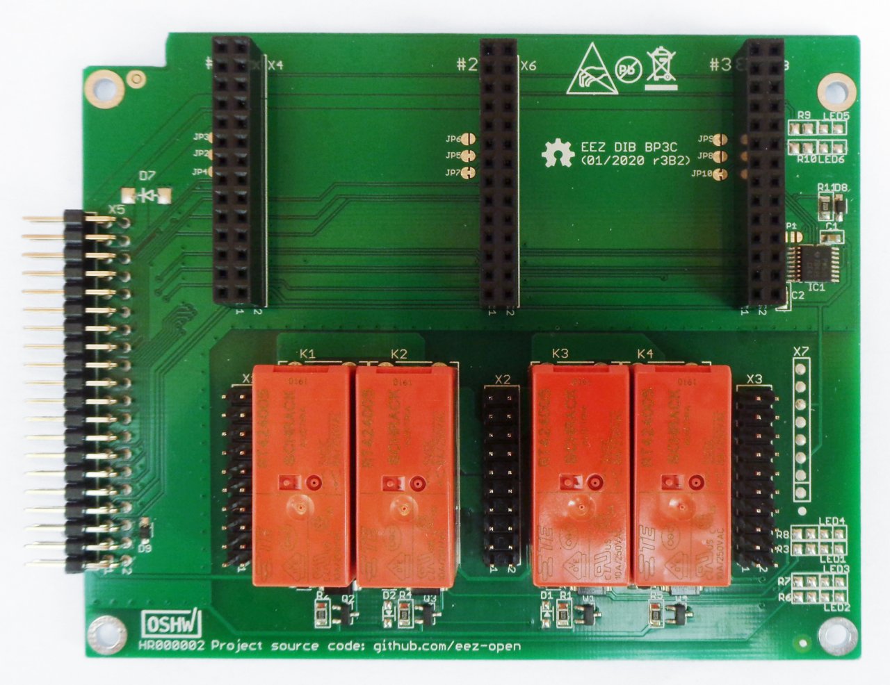
The BP3C backplane follows the DIB v1.0 specification and accepts up to three DIB peripheral modules that could be of power sourcing types such as DCP405 power module hence it also provides 20-pin power sourcing 0.1” pin headers. The MCU board 40-pin connector is located on side for mounting the MCU board horizontally in the same line with the backplane.
Power sourcing outputs coupling
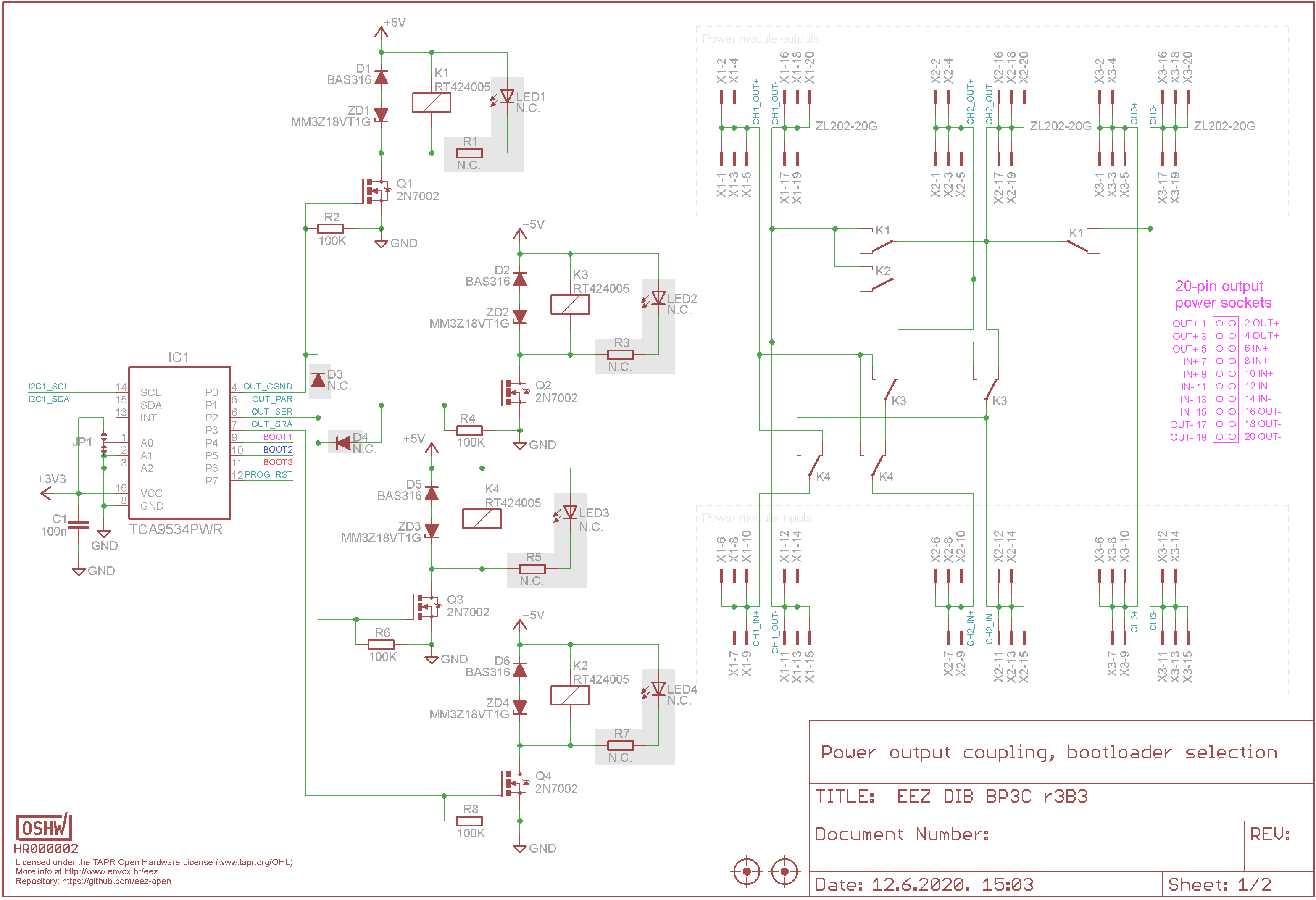
Four different types of power sourcing module outputs is possible with this backplane thanks to four on-board power relays that are controlled with I2C 8-port I/O expander (IC1) as shown on Fig. 3. Coupling of power outputs under MCU control has the following benefits:
- External wiring and lousy and inadequate connections are avoided. Therefore additional voltage drop is not introduced and that lowers the chance of damaging the load by wrong wiring.
- Coupling is performed under controlled and safe conditions, i.e. when coupling is initiated, the affected channel outputs are disabled first and set output voltages and currents are reset to zero values.
- When coupling is affecting voltage or current ranges as in case of coupling in series or parallel, control of the coupled boards can be unified to decrease possibility for user mistakes due to output values misreading e.g. single value output voltage of +62.8 V will be displayed instead of two separated +31.4 V values, that one do not need to guess actual value. The same is valid for setting output value (voltage, current or power).
- Power boards which outputs are coupled in series or parallel are utilized equally, e.g. when current is set to 8 A, each channel will be set to 4 A. Likewise when output voltage is set to +70 V, each channel will be set to +35 V. Additionally, balancing algorithm deployed in firmware takes care about output voltage and current when operating mode is changed due to change in load. Check this video for more information about coupled outputs balancing.
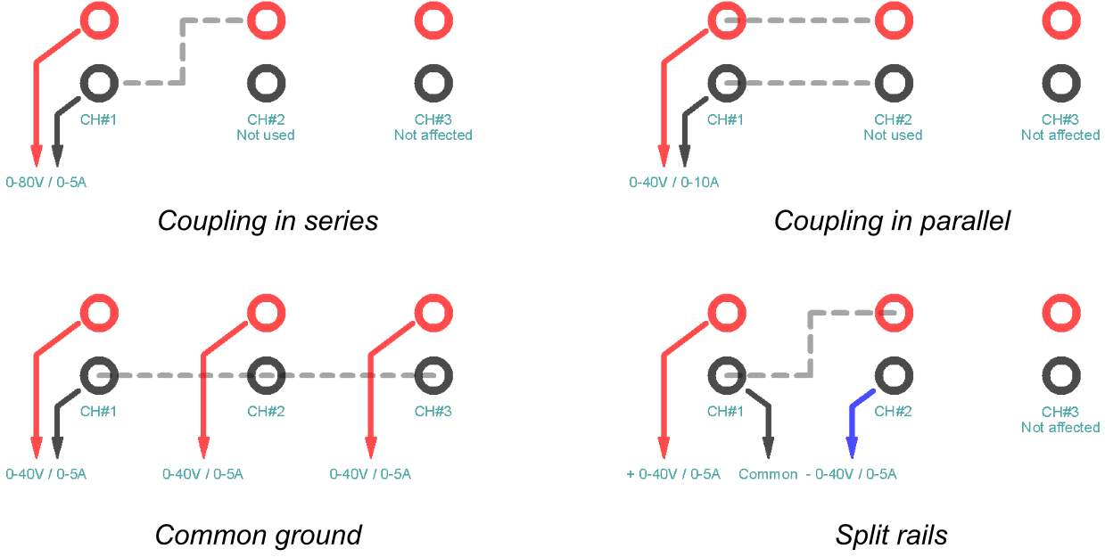
The power sourcing modules outputs can be coupled in one of the following way (see Fig. 4.):
- Coupling in series outputs of the first two channels to double voltage range. The active output become Ch#1. Ch#3 output remains unaffected
- Coupling outputs of the first two channels in parallel to double current range. The active output become Ch#1. Ch#3 output remains unaffected
- Common GND, when all channel Out- terminals are connected together
- Split rails when Ch#1 Out- and Ch#2 Out+ are connected. The Ch#1 Out+ become positive rail, and Ch#2 Out- negative rail.
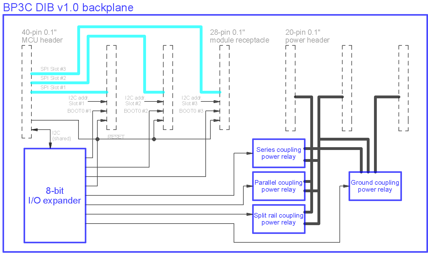
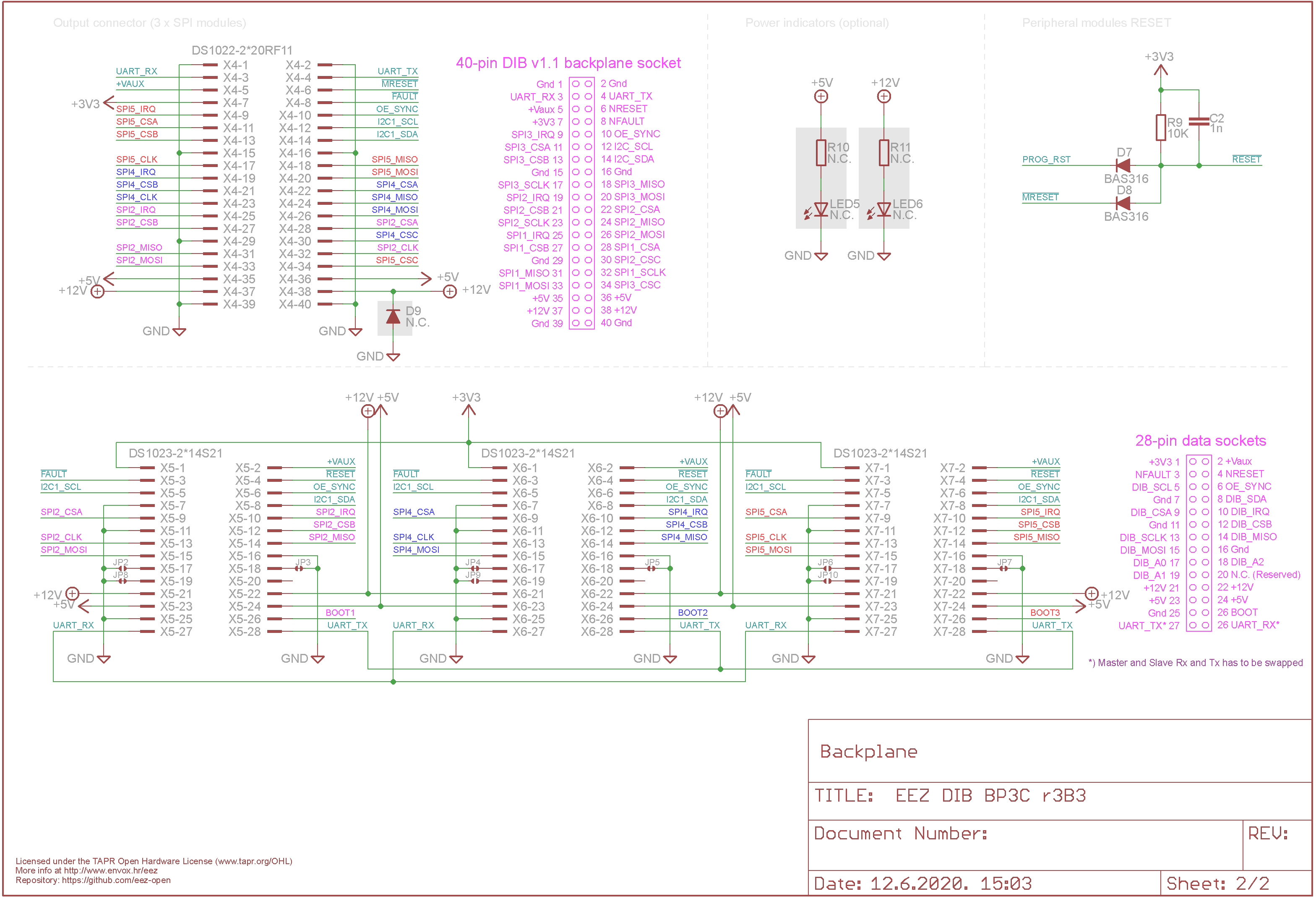
The MCU 40-pin right angled 0.1” pin header and three peripheral module 28-pin 0.1” receptacles wiring is shown on Fig. 5. All three peripheral modules share the same I2C bus (SSDA, SSCL) and async UART, but have a dedicated SPI buses, together with two device select inputs (CSA, CSB) and interrupt outputs (IRQ).
Note that A0-A2 module identification pull-up inputs are assigned to addresses 1 (001), 2 (010) and 3 (011) respectively by selective grounding (for “zero” value).
NRESET, NFAULT and SYNC signaling are also shared among all peripheral module connectors. The same is true for power inputs: +5V, +12V, +3.3V (low-power, max. 20 mA) and +VAUX.
Bootloader control
Peripheral module could comes with on-board MCU. Therefore its firmware has to be uploaded from time to time with new releases and that require some sort of connection (i.e. JTAG, USB, UART) with a programmer. Other possibility is to use master MCU from the MCU board to perform firmware upload of the on-board (slave) MCU using one of the buses (UART, I2C or SPI) available on the backplane.
To initiate firmware upload slave MCU could require on startup to enter specific mode of operation when built-in bootloader will be activated and take care about firmware code writing into internal flash memory. The BP3C provides dedicated BOOT signal for each module that master MCU can select which module is going to be programmed. Additionally, since MCU’s BOOT input has to be set on the power up or reset, an I/O expander output (PROG_RST) is “OR”-ed (D7, D8) with master reset (MRESET) that master MCU can reset peripheral modules after set BOOT output of the target module without need for input power recycling.
PCB layout
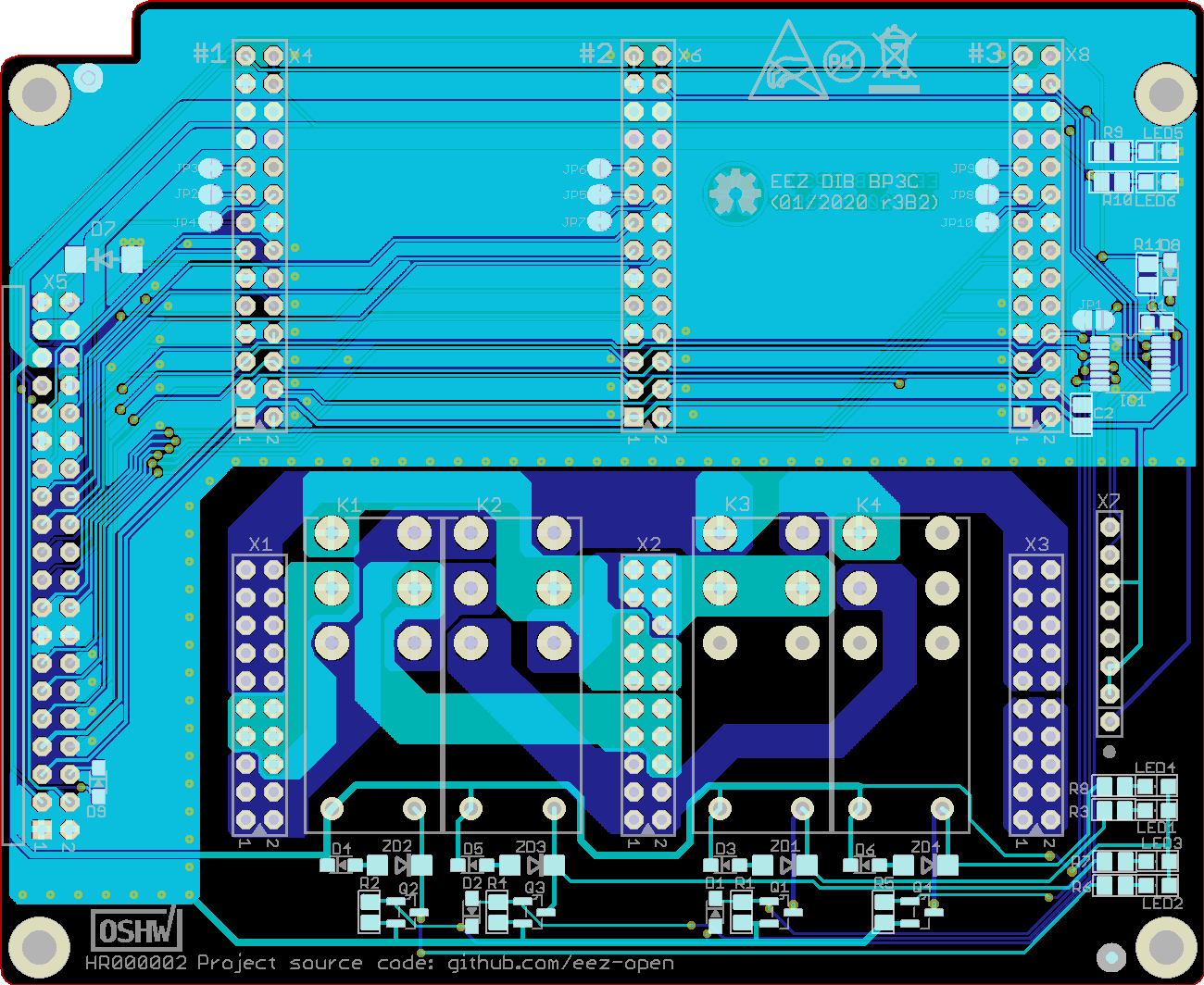
The BP3C backplane is assembled on the 110 x 90 mm 2-layer PCB. Coupling relays are located between 20-pin power sourcing pin headers with proper distance that their height does not interfere with components on the power sourcing module such as DCP405 or DCM220. Although peripheral module connector’s A0-A2 inputs are keyed on the PCB to provide addresses 1, 2 and 3 that default addressing could be changed by modifying PCB jumpers (JP2-JP10).

