EEZ DIB STM32F7 MCU module
|
Current version |
r3B3 |
|
Status |
Ready for production |
|
PCB manufactured |
Yes (r3B3) |
|
PCB assembled |
Yes (r3B3) |
|
BOM |
Yes (TME, Mouser, Digikey, Farnell, RS) |
|
File repository |
https://github.com/eez-open/modular-psu/tree/master/mcu |
|
License |
|
|
Contributions |
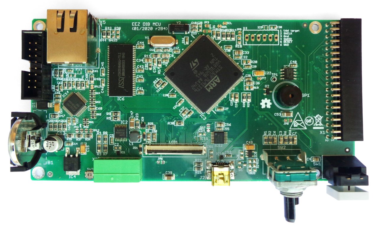
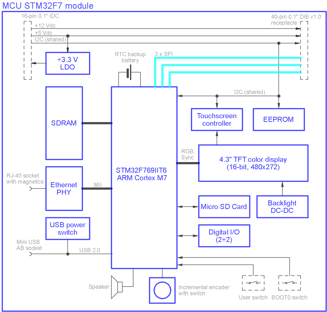
The MCU board provides main processing powers that can be shared between peripheral modules inserted into DIB backplane. Its also in charge for connectivity with PC using USB FS and 10/100 Mbit/s Ethernet. Finally, it provides HMI that include 4.3” TFT LCD with resistive touchscreen, rotary encoder and an user switch with programmable function.
Feature list
- STM32F769IIT6 32-bit ARM Cortex®-M7 MCU, 216 MHz, 2 MiB Flash, 512 KiB SRAM, LQFP-176 package
- Digital I/O: 2 x buffered inputs and 2 x buffered outputs (alternative functions: UART, PWM out)
- Rotary encoder with switch
- 1 x user switch
- 3 x SPI channels (2 x Chip selects per channel), 40-pin IDC connector (DIB v1.0)
- Battery backup (CR2032 button cell type)
- USB FS OTG
- Micro SD card
- DP83848C Ethernet PHY (10/100 Mbit/s)
- 32 KiB I2C EEPROM
- SWG/JTAG connector (optional)
- 8 MiB SDRAM (e.g. IS42S16400J)
- TFT LCD 0.5 mm FFC 40-pin connector (e.g. 4.3” RFE43BH-AIW-DNS or RFE430Y-AIW-DNS)
- TFT backlight brightness control
- Resistive touch controller
- Soft-start/stand-by control lines for AUX power supply
- Small on-board speaker
- Input power: +5 V (+12 V pass-thru to peripheral modules)
- On board +3.3 V LDO
- Bootloader input (BOOT0) and jumper (optional)
- Dimensions: 139 x 70 mm, 4-layer PCB
Selected STM32F769IIT6 is a high performance 32-bit RISC core MCU operating at up to 216 MHz frequency. The Cortex®-M7 core features a floating point unit (FPU) which supports Arm® double-precision and single-precision data-processing instructions and data types. It also implements a full set of DSP instructions and a memory protection unit (MPU) which enhances the application security. It comes in various size and packages, and LQFP176 package is chosen since it offers enough pins for above listed features and it can be soldered manually on the PCB.
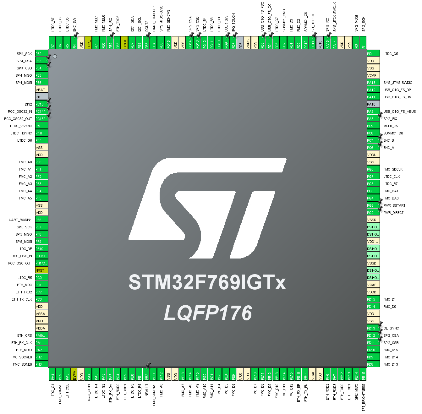
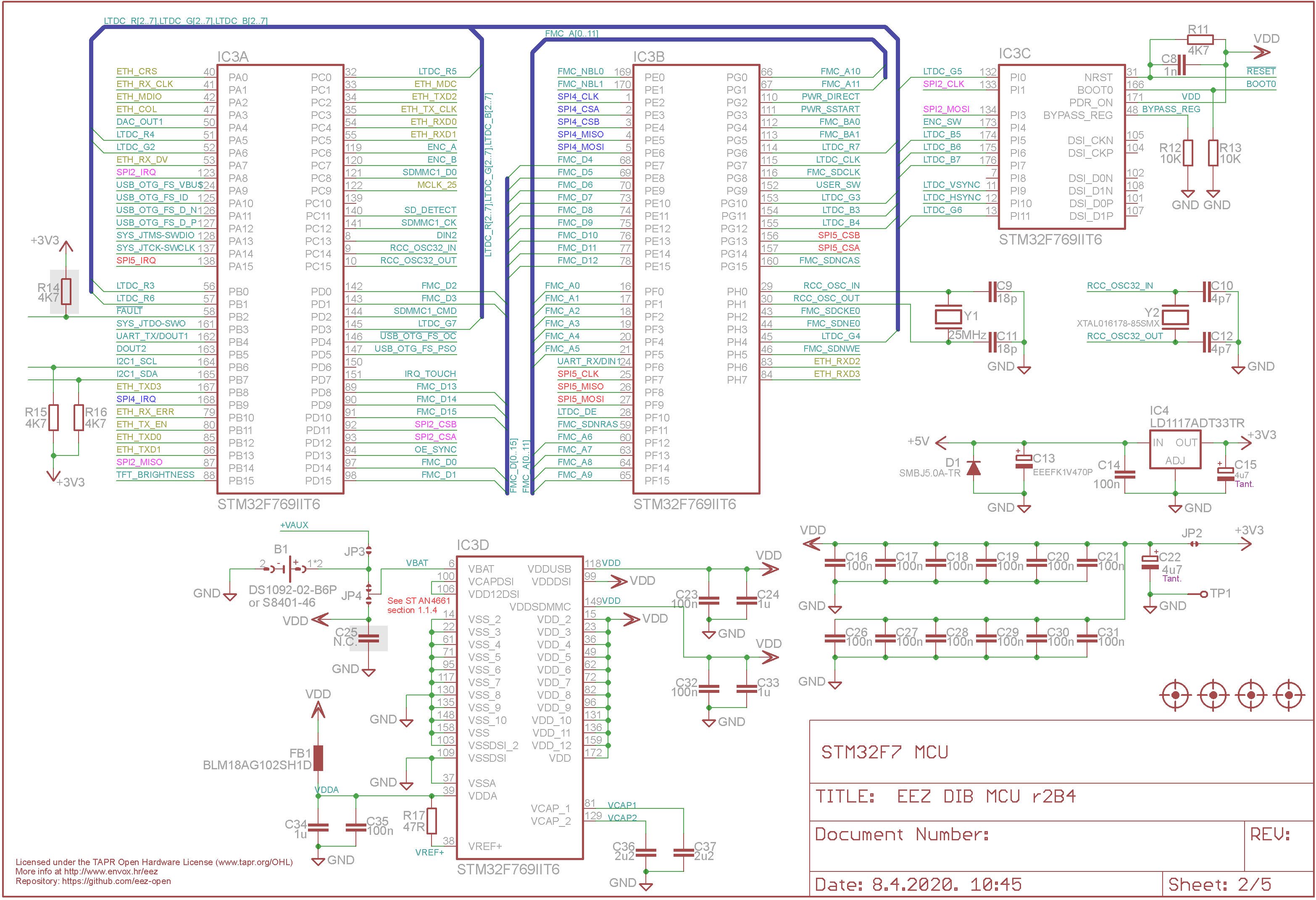
The pin assignment is shown on Fig. 3. generated with CubeMX tool. The latest revision can be found on the GitHub. As it is visible from pin assignment, the MCU directly provides the most of the functionalities mentioned above. The MCU (IC3) wiring is shown on Fig. 4. and only four pins (PI8, PA10, PC10, PD6) and bus for a DSI type of display left unassigned.
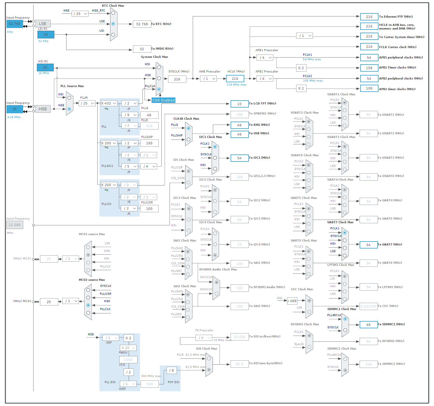
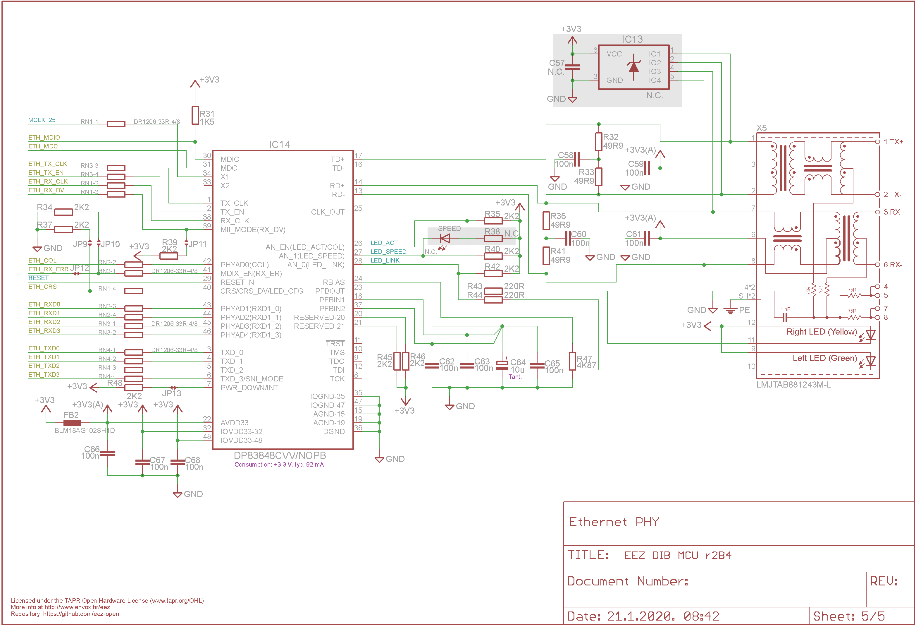
On-board LDO (IC4) is deployed to step-down from +5 V to its working voltage of +3.3 V. A bank of decoupling capacitors (C16-C21 and C26-C31) are located as close as possible to VDD input pins. The main clock (HSE) frequency is set with 25 MHz XTAL (Y1). Another 32.768 KHz XTAL (Y2) is required for internal RTC (real time clock) so it can remain functional when power is switched off and backup power (coin batter in B1 holder) is used. The MCU clock settings is shown on Fig. 5. Relatively high main clock frequency of 25 MHz is intentionally selected to drive directly Ethernet PHY (IC14 on Fig. 9.) using the MCLK_25 output (PC9 pin). Frequency prescalers are set to provide max. allowed MCU frequency of 216 MHz.
Connectors, Digital I/O rotary encoder and user switch
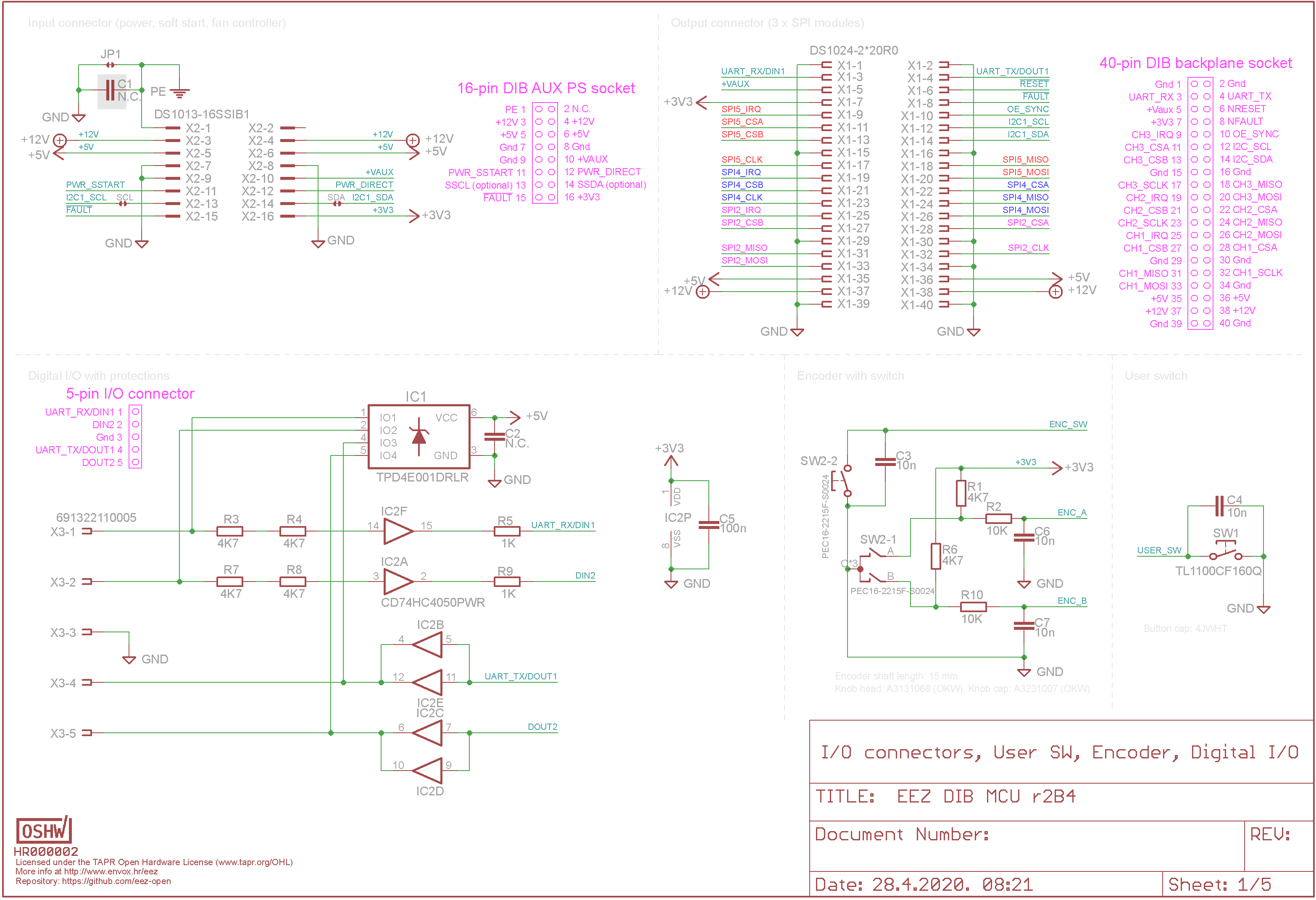
The MCU board uses two connectors (see Fig. 6.) in accordance with DIB v1.0 specification: 40-bit angled 0.1” receptacle (X1) is intended for direct connection with the BP3C backplane, while 16-pin angled IDC (X2) is used for flat cable connection with AUX power supply.
Two protected digital inputs and outputs lines are provided for MCU’s communication with external devices. Input lines are protected with resistors (R3+R4, R7+R8) connected in series with digital buffers (IC2), which outputs are additionally dampened with resistors (R5, R9) to reduce possibility of MCU damage. IC2 inputs accept voltages up to +5.5 V. Therefore, it acts as level translator if inputs are driven with TTL levels. Digital outputs are boosted with two pair of buffers wired in parallel to provide higher current capacity. Finally, all inputs and outputs are clamped for additional safety with low capacitance 4-channel ESD-protection device (IC1).
On-board rotary encoder (SW2) is equipped with push-button and is supplemented with tactile switch (SW1) which can be assigned to various functions to provide more flexibility in interactions with user.
On-board memory and SWD interface
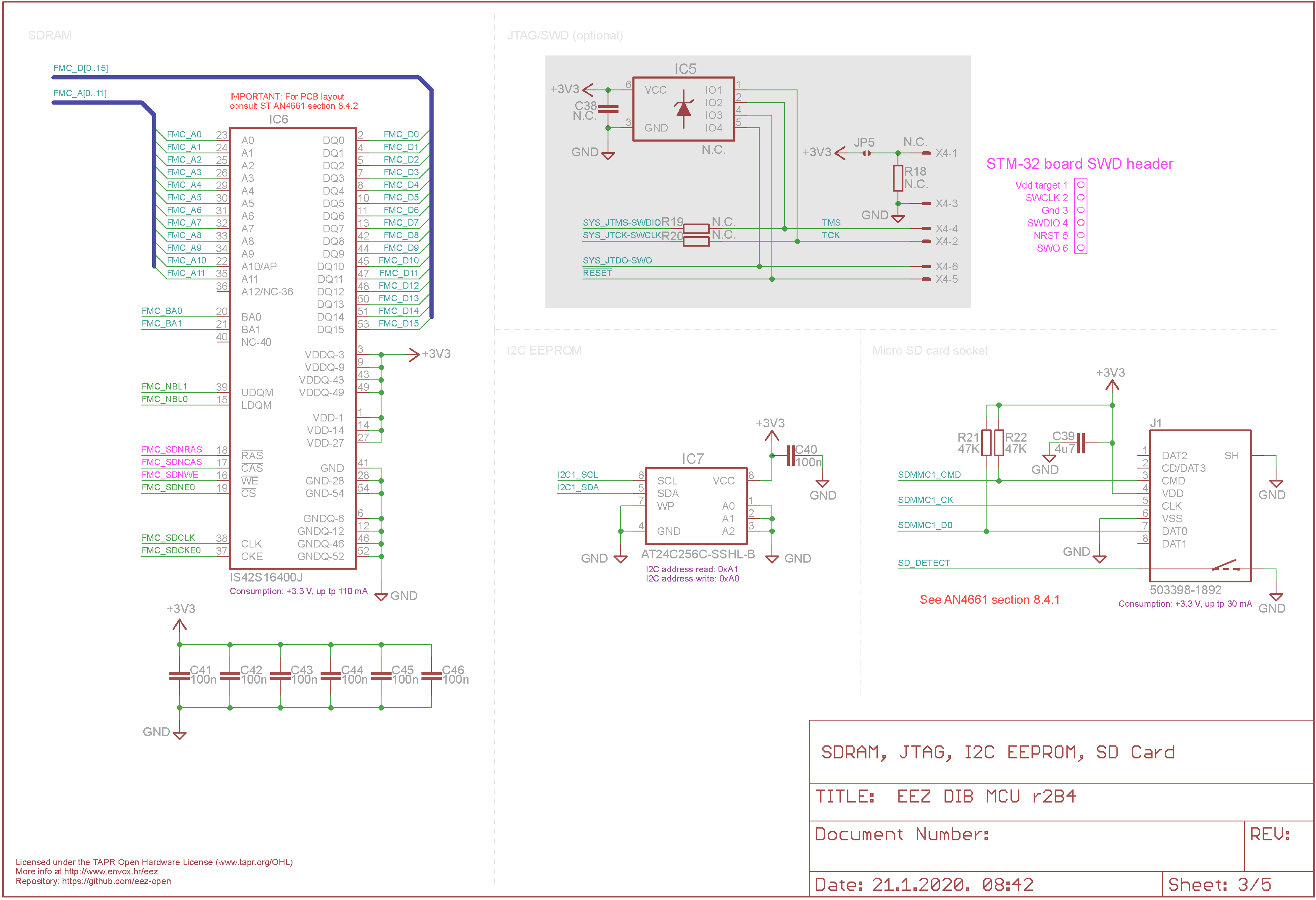
The MCU board has three different memory devices (Fig. 7.):
- SD-RAM (IC6) managed by FMC (Flexible Memory Controller) with 12-bit address bus and 16-bit data bus,
- EEPROM (IC7) connected to shared I2C bus
- Micro SD card inserted into “push-push” card holder (J1) managed by three lines SDMMC (SD Memory Management Controller). Additional input (SD_DETECT) is used for detecting presence of the micro SD card.
Optional SWD interface for programming and debugging purposes is provided by ESD protected (IC5) 6-pin 0.1” pin header (X4). Its pinout is compatible with STlink debugger that can be found on evaluation boards and kits such as Nucleo and Discovery.
If an STlink debugger is to be used, resistors R19 and R20 (22 – 47 Ω) will also need to be installed.
TFT display, touchscreen, USB, speaker and BOOT0 switch
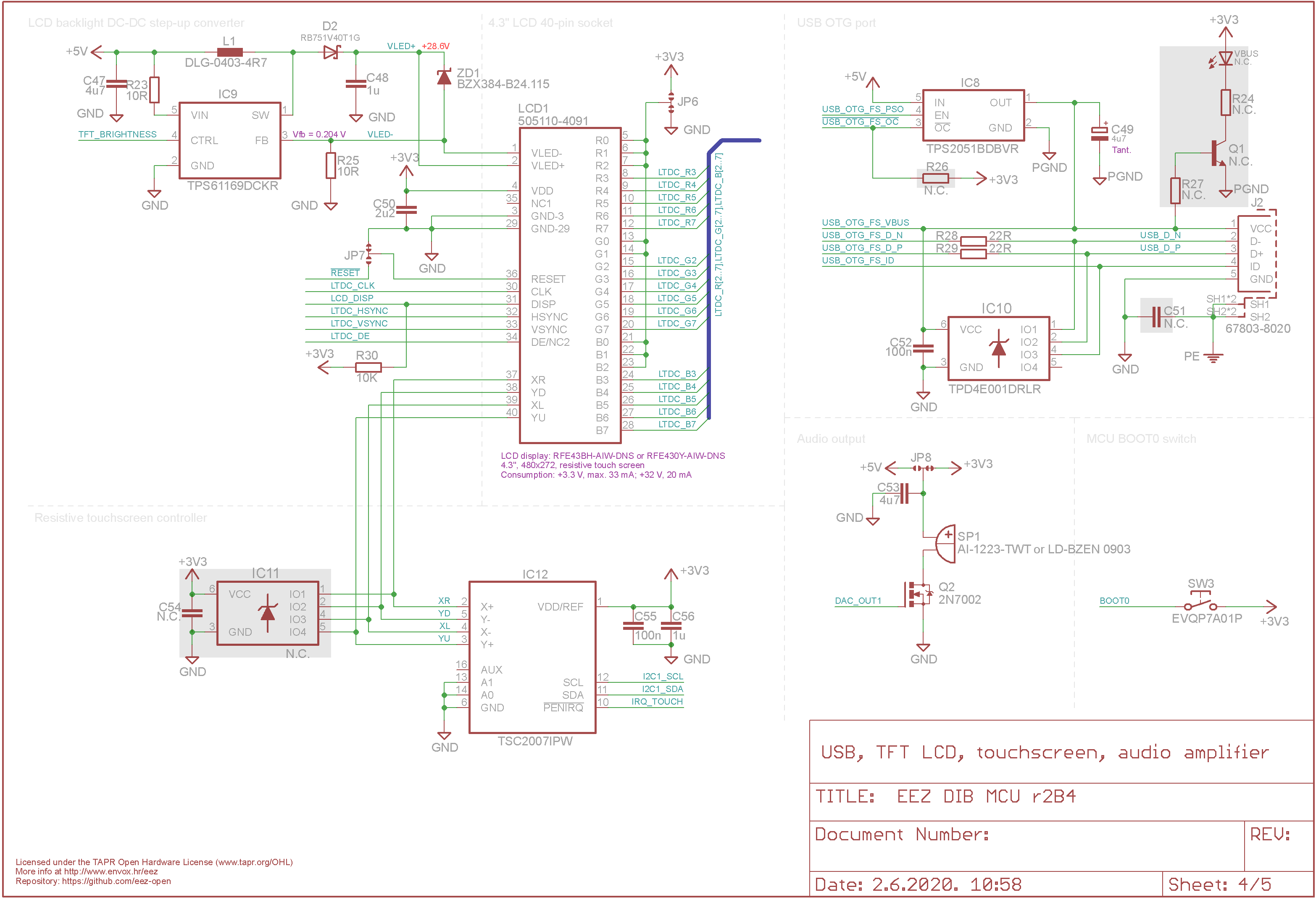
The MCU is capable of driving directly a TFT display with RGB interface generating all required signals and pixel data up to 24-bit format. However, only 16-bit RGB interface is used due to pin limitations of selected package and pin demands by other activated features. First two bits of all color channels can be set to 0 (default) or 1 using PCB jumper (JP6). A standard 40-pin 0.5 mm FFC ZIF connector (LCD1) is used for interfacing TFT display and resistive touchscreen. The MCU board is tested with EastRising ER-TFT043-8-3023 and Raystar RFE43BH-AIW-DNS, 4.3” 480 x 272 pixel displays.
TFT LED backlight requires high voltage (~30 V) power supply with constant current output. TPS61169 (IC9) WLED driver (boost type) serves this purpose. It comes with built-in protection against open circuits to prevent the output voltage from exceeding the absolute maximum voltage ratings of the device. Additionally, a Zener diode (ZD1) is mounted to protect TFT LED array, by keeping the output voltage within safe limit. Output current is programmed with R25 and CTRL input is used for brightness control that is connected to PWM output (TFT_BRIGHTNESS).
Touchscreen functionality is accomplished with TSC2007, a 4-wire controller with I2C interface (IC12) and belongs to one of the few models that comes in package with exposed pads (for simple manual soldering) and is still in production. It includes 12-bit SAR ADC (can be downsized to 8-bit for shorter conversion time) and drivers and the control logic to measure touch pressure. Since TSC2007 has built-in ESD protection, IC11 is not mounted, and marked as optional.
The USB interface is also directly provided by MCU that can be programmed to act as USB device or host with OTG capability over 5-pin USB AB mini socket (J2). USB power distribution (max. 500 mA) in host mode is controlled with IC8 and all data lines that is protected against ESD with IC10. Optional LED (VBUS) indicates USB VBUS voltage.
A sound generated by DAC (DAC_OUT1) is simply buffered with Q2 which drives PCB mounted small 8 Ω loudspeaker (SP1). Speaker power supply can be set with PCB jumper (JP8) to +3.3 V (default) or +5 V.
The BOOT0 switch (SW3) is used to enable MCU’s embedded bootloader that is stored in the internal boot ROM memory (system memory) of STM32 devices during the power up. Bootloader main task is to download the application program to the internal Flash memory through one of the available serial peripherals such as USB when DFU protocol can be used.
Ethernet PHY
The MCU provides 10/100 Mbit MAC with dedicated DMA and can work with IEEE 1588v2 hardware. Yet, it does not offer physical layer (PHY) interface, thus an external PHY transceiver, DP83848C (IC14) is incorporated. The DP83848 can be interfaced with both MII and RMII, and MII is chosen because of lower reference clock frequency (25 MHz for 100 Mbit/s, instead of 50 MHz for RMII) despite the higher pin count. It has Auto MDIX capability to select MDI or MDIX automatically and supports Auto-Negotiation for selecting the highest performance mode of operation. Connection with Ethernet network infrastructure is accomplished using RJ-45 socket (X5) with integrated magnetics (i.e. impedance/isolation transformers). Its interface lines can be additionally protected with optional IC13.
The Ethernet socket is connected by a short patch cable to the enclosure rear panel.
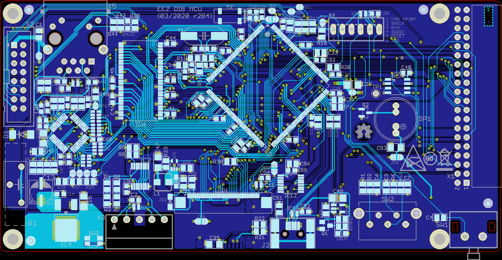
The MCU board is assembled on the 139 x 70 mm 4-layer PCB. The PCB is designed in such a way that all connectors and devices which require interaction with user: i.e. BOOT0 switch, Digital I/O, TFT, MicroSD card socket, USB, rotary encoder and user switch are positioned to the same PCB edge. Therefore, when properly mounted, they can be easily accessed from the EEZ BB3 enclosure’s front panel. Only the TFT display will require additional mounting frame or it can be fixed with the mounting tape.
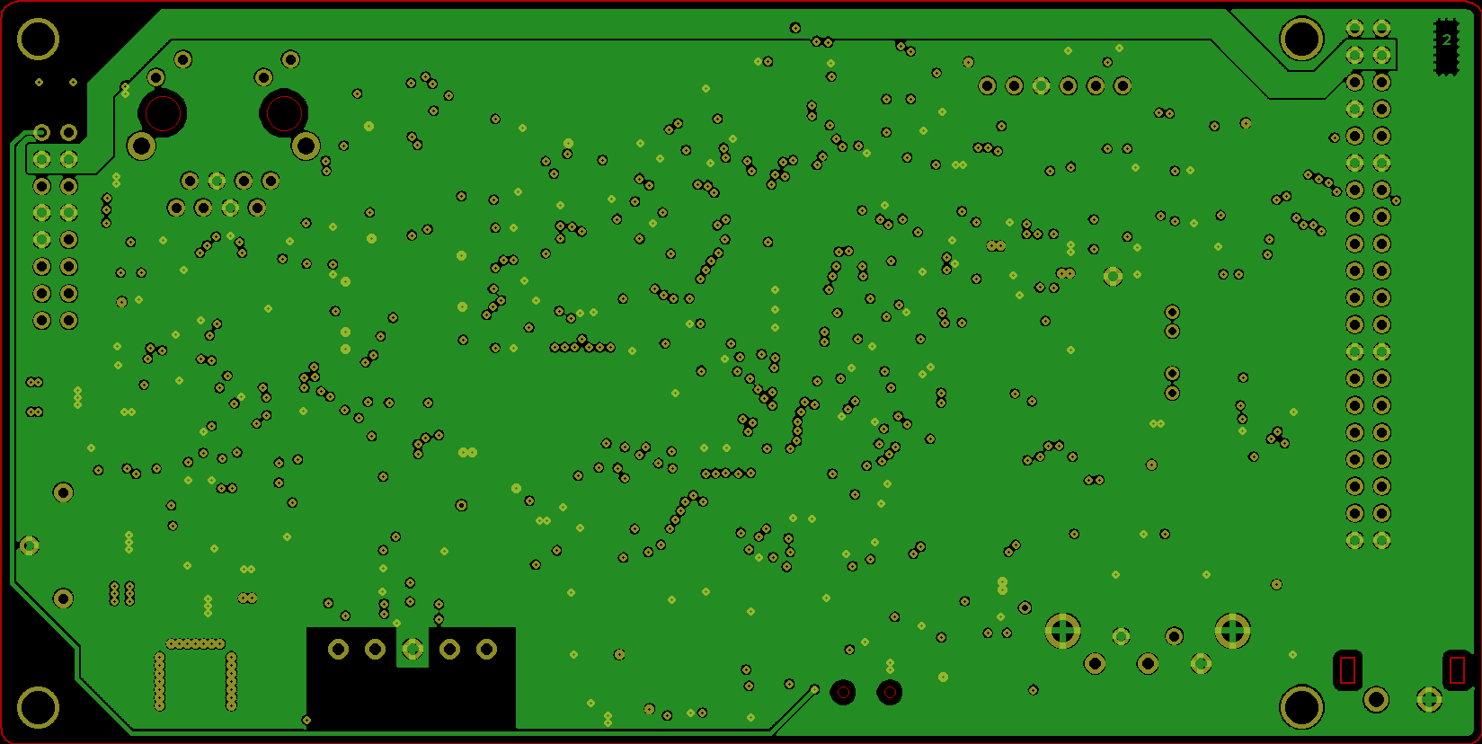
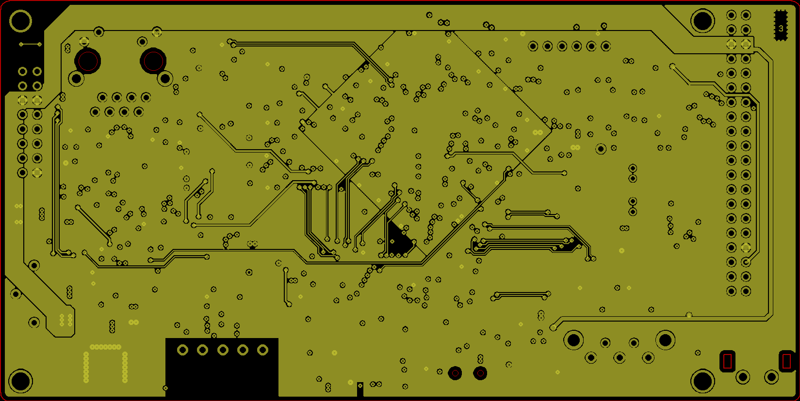
PCB’s top and bottom layers are used for signal routing, while two internal layers are used as ground and voltage planes. A special attention was needed to route SDRAM and Ethernet PHY with MCU. The same is valid for the USB data lines that should be routed as differential pair with matched impedance to 90 Ω.

