| Current version |
r1B4 |
| Status |
Completed, ready for production |
| PCB manufactured |
r1B2 |
| PCB assembled |
r1B2 |
| BOM | |
| File repository | |
| License | |
| Contributions |
Feature list
- 24-bit 4-channel simultaneous sampling ADC with SPI
- AIN#1: Hi-voltage isolated (floated) input, 2 measurement ranges (±50 V, ±480 V)
- AIN#2: Hi-current isolated (floated) input, 2 measurement ranges (±1 A, ±10 A)
- AIN#3: Hi-voltage input, 3 measurement ranges (±2.4 V, ±12 V, ±240 V)
- AIN#4: Hi-current input, 3 measurement ranges (±24 mA, ±500 mA, ±10 A) share common GND with AIN#3
- Latching relays for lower continuous power consumption
- On-board ±2.5 V low noise LDOs
- Optional external voltage reference
- Dimensions: 132 x 68.5 mm, 4-layer PCB
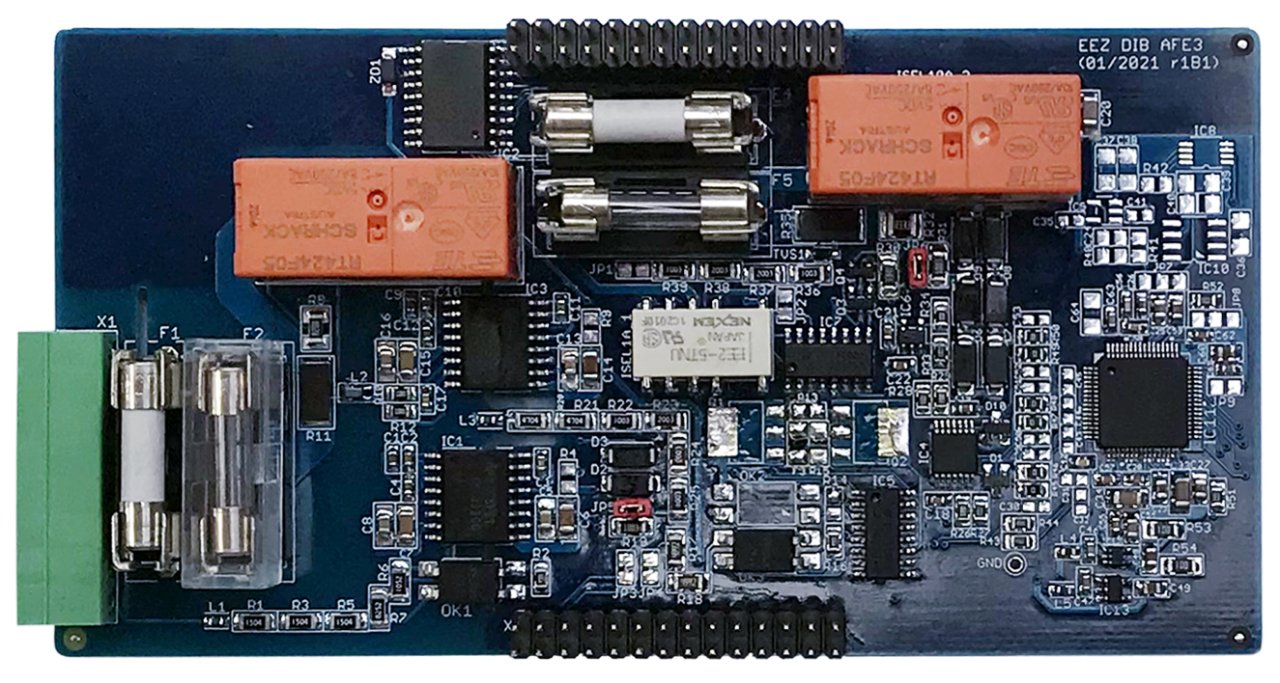
The AFE3 is an expansion board for the MIO168 that offers four analog inputs that are simultaneously sampled up to speeds of 16 KSPS (24-bit) or 32 KSPS (16-bit). Two fully isolated inputs, one for voltage measurement and the other for current measurement make it suitable for power measurement, and in combination with the remaining two inputs for efficiency measurement and for devices that have galvanically isolated primary and secondary side (AC/DC, DC/DC converters, inverters, chargers, etc.).
The AFE3 inputs are exposed to the front panel via an 8-pin connector with a 3.81 mm pitch (X1). The AFE3 is connected to the MIO168 module using two 28-pin connectors with a 2.54 mm pitch (X2, X3) through which all control and power lines come.
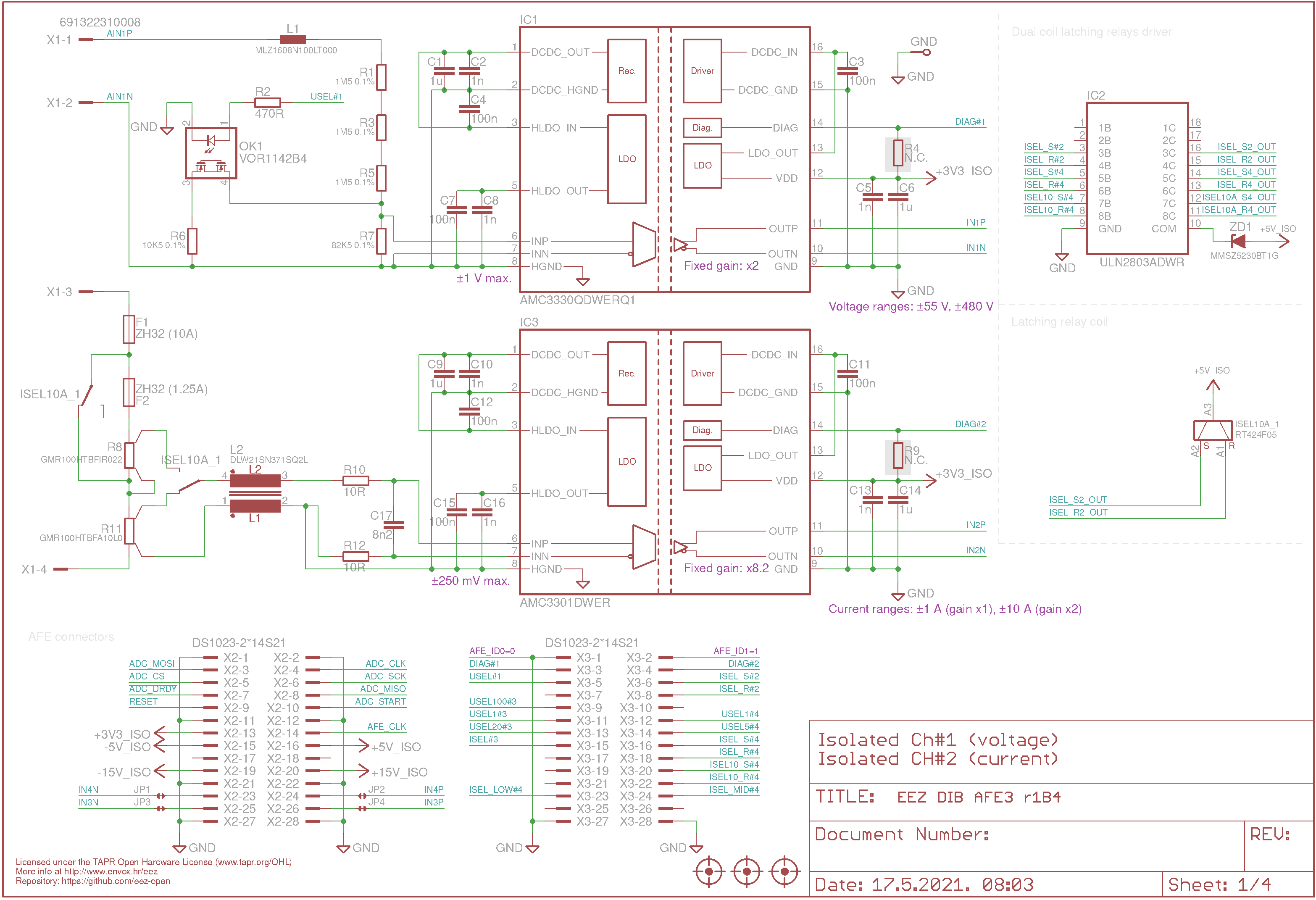
The separation of the first two inputs was made using precision reinforced isolated amplifiers with integrated DC/DC converter (IC1, IC3), as shown in Fig. 2.
The first input (AIN1) is intended for voltage measurement in two ranges of up to ± 50 Vdc (35 Vrms) or ±450 Vdc (320 Vrms). The measuring range of the isolated amplifier IC1 is ±1 V with a gain of x2 which leaves enough headroom for the ADC input whose measuring range is ±2.4 V. Voltage range selection control must also be isolated and optoMOSFET OK1 is used which changes the attenuation of the voltage divider by adding R6 for the high range.
Isolated current measurement is possible at the AIN2 input. Since this input is isolated from AIN1 no special care should be taken about the wiring (i.e. where the “hot” side of the voltage and current is connected) and it is possible to have low- and high-side current measurements.
The measuring range of the isolated amplifier IC3 is ±250 mV with a fixed gain of x8.2. With the selected current shunts we will have voltage drops of up to ±230 mV (R8 + R11) for 1 A range or ±100 mV (R11) for 10 A range. Therefore at the ADC input we will have voltages of ±1.89 V for the low range and ±820 mV for the high range which can be further amplified by setting the ADC PGA to 2.
Due to the large current for switching current ranges, a power relay ISEL10A_1 is used, which is of the latching type in order to reduce the total continuous consumption of the module. Two outputs from the Darlington driver (IC2) are used to control it.
The AIN2 input is protected with two fuses (F1, F2) that to some extent increase the burden voltage which will be more noticeable at high range but add the necessary protection against extreme loads.
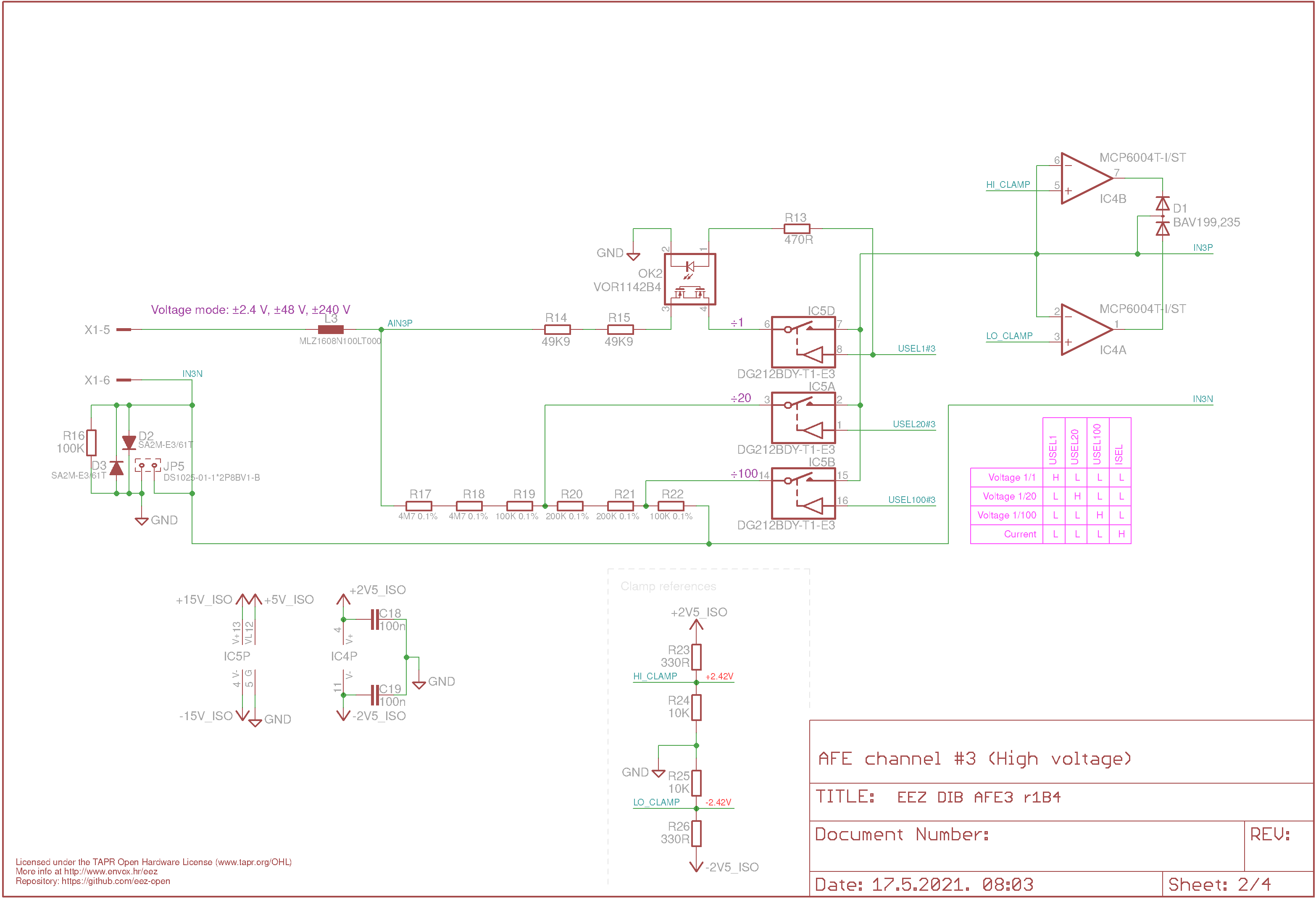
AIN3 is intended for voltage measurement in three measuring ranges: ÷1 (± 2.4 V), ÷20 (±48 V) and ÷100 (±240 V). This is solved by using a voltage divider with multiple outputs that are selected using analog switches (IC5). Allowable voltages on analog switches are up to ±15 V, so for this reason it was necessary to separate ÷1 input with an OptoMOSFET (OK2) that can withstand input voltages up to 600 V.
Analog switches and OptoMOSFET are directly controlled by the MCU on the MIO168 module.
The input to the ADC is further protected by using an active clamp with an operational amplifier (IC4) and ultra low leakage diodes (D1). Clamping voltage is set with two dividers R23, R24 for positive and R25, R26 for negative voltages.
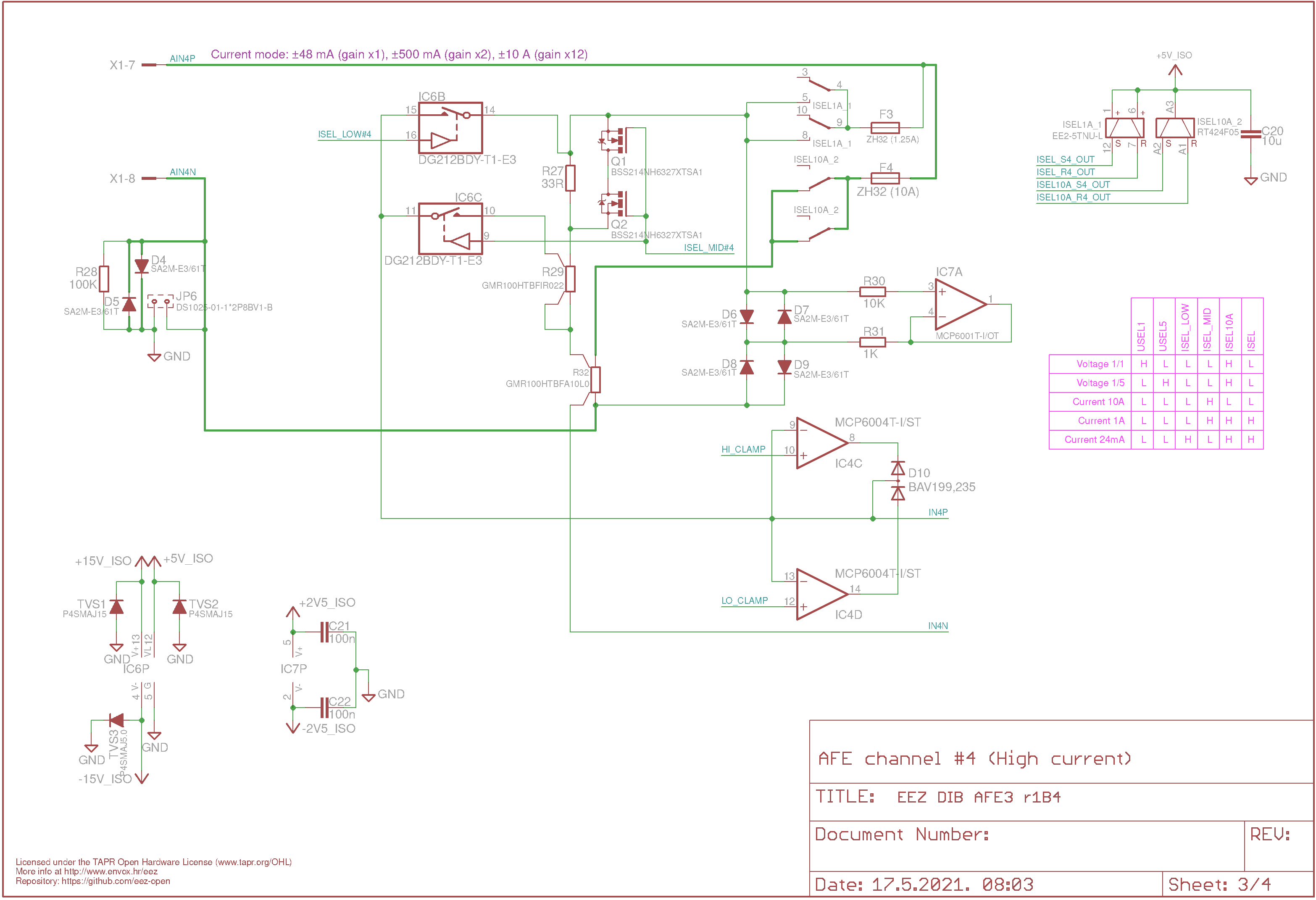
AIN4 is intended for measuring current in three measuring ranges: ±24 mA, ±500 mA and ±10 A. Current switching for Mid- and High-range uses power relays (ISEL1A_1 and ISEL10A_2), also of the latching type for lower consumption. The voltage selection on the current shunt is carried out with analog switches (IC6), and to reduce the burden voltage in the Mid-range a bypass with MOSFETs (Q1, Q2).
Fuses F3 (Mid-/Low-range) and F4 (High-range) are used for over-current protection. Additional protection of Low- and Mid-range current shunts was performed with a circuit consisting of diodes D5-D9 and operational amplifier IC7.
Similar to AIN3, The input to the ADC is protected by using an active clamp with an operational amplifier (IC4) and ultra low leakage diodes (D10).
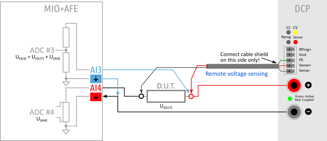
Unlike AIN1 and AIN2 which are isolated from each other, AIN3 and AIN4 share the same GND so care should be taken when connecting them if power is to be measured. Generally speaking care should be taken that connecting the GND of the AIN3 (voltage input) does not lead to a bypass of the AIN4 current shunt. Such a situation can be avoided by connecting as in Fig. 5., where the current is measured at low-end so AIN3 and AIN4 GND inputs can be wired together externally.
Please note that although AIN3 and AIN4 share a common GND with each other and with the GND of the MIO168 module, they are still “floating” with respect to the MCU’s (BB3 chassis) GND. Such isolation is achieved on the MIO168 module, not on the AFE expansion board itself.
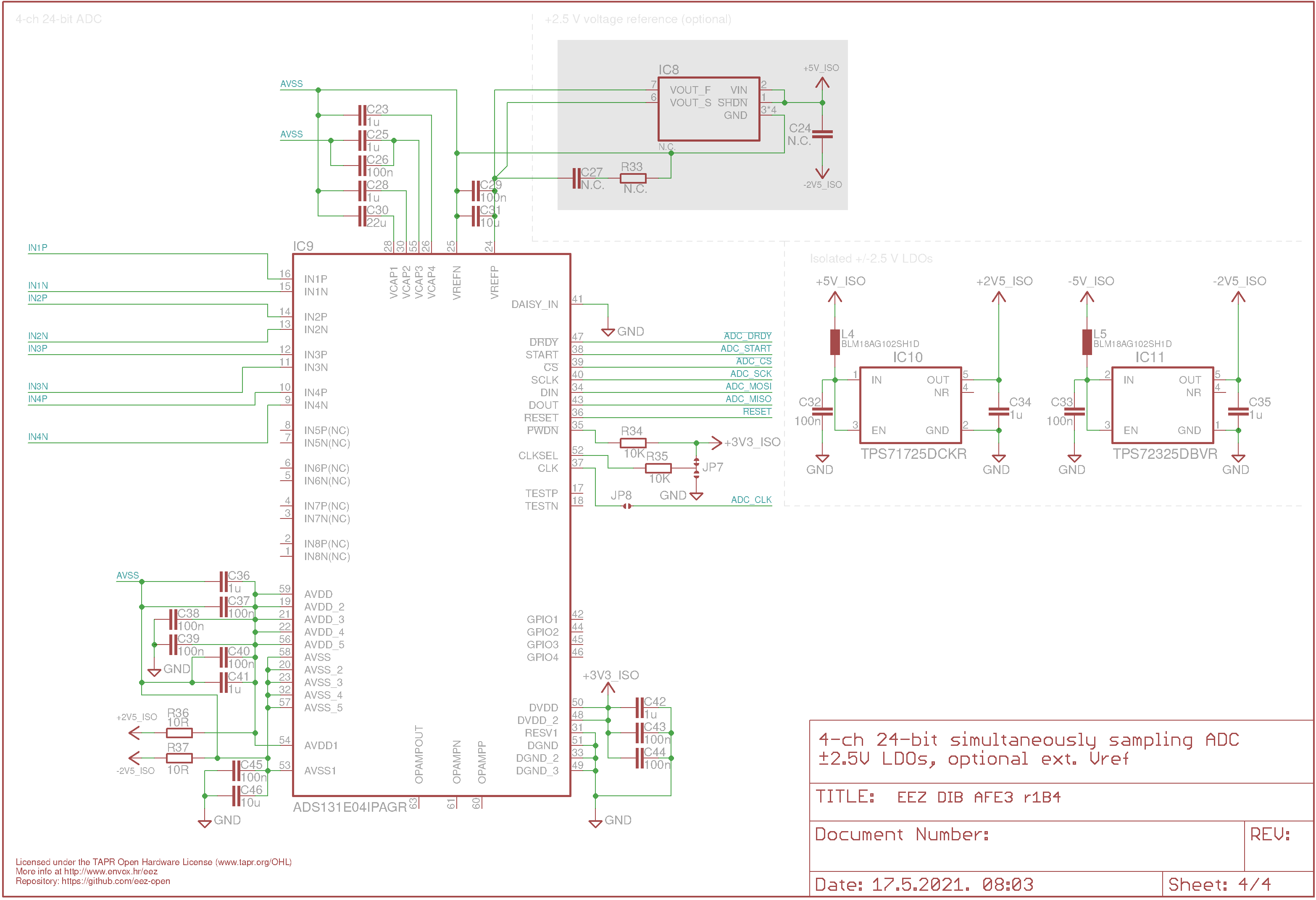
For A/D conversion, a 4-channel 24-bit ADC (IC9) is used that allows simultaneous conversion on all channels. The ADC comes with an internal clock oscillator and a precise voltage reference (temperature drift of 20 ppm/°C). Optionally, an external voltage reference (IC8) LTC6655-2.5 (low drift: 2 ppm/°C, high accuracy: ±0.025%) can be mounted on the PCB if better performance is required.
In order for the ADC to be able to accept the bipolar signal at the input, a split rail power supply is used for which two low noise LDOs (IC10, IC11) are used to obtain ±2.5 V.

