| Current version |
r2B5 |
| Status |
Completed, ready for production |
| PCB manufactured |
Yes (r2B5) |
| PCB assembled |
Yes (r2B5) |
| BOM |
Yes (TME, Mouser, Digikey, Farnell, RS) |
| File repository |
https://github.com/eez-open/dib-mio168 (include Eagle, Gerber and BOM files) |
| License | |
| Contributions |
Feature list
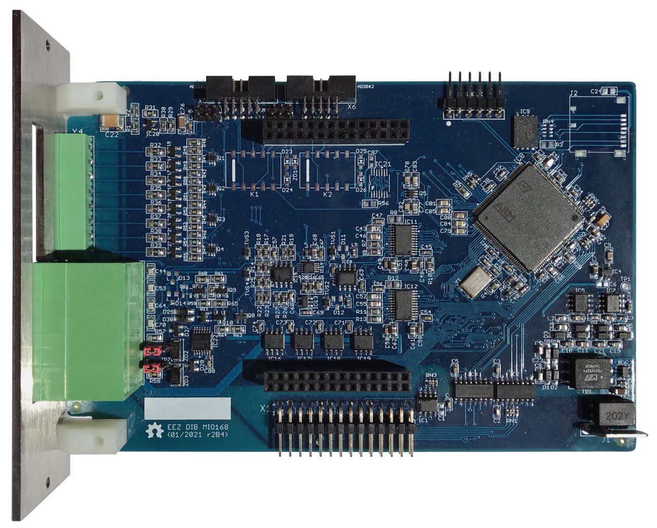
- On-board STM32F446ZCT6 high-performance foundation line MCU, ARM Cortex-M4 with DSP and FPU, 256 KiB Flash, LQFP-144 package
- 1 x 8-pin single row 3.81 mm connector (digital inputs)
- 1 x 16-pin dual row 3.81 mm I/O connector (digital and analog outputs)
- 2 x 10-pin ADIB 2.0 mm connectors
- 8 x protected digital inputs (+3.3/5, +12/24 V), 2 x fast/slow, 6 x slow
- 8 x digital outputs (low-side) with multiple protections and FAULT detection, 550 mA per channel (current limit 1 A)
- 2 x PWM outputs (protected) or sensor bias power (±15 V, max. 10 mA)
- 2 x analog bipolar outputs (±5 V, ±10 V, 0-5 V, 0-10 V, 4-20 mA, 0-20 mA, 0-24 mA). Voltage or current output with protection. 12-bit DAC, replaceable with pin compatible 16-bit version
- 2 x analog bipolar outputs ±10 V. 12-bit DAC, replaceable with pin compatible 14- or 16-bit version
- On-board isolated power supply with ±5 V outputs (with 4x multipliers), ±15 V and +3.3 V LDO
- Firmware download via SPI
- Optional SWD for debugging
- Optional Micro SD card
- I2C EEPROM for storing board specific parameters
- Dimensions: 146 x 95 mm, 4-layer PCB
The MIO168 is a versatile module that offers multi-channel generation and measurement of digital and analog signals. In the basic version it offers 8 digital 2-level inputs and 8 low-side high current switches. It additionally offers two bipolar voltage or current analog sources and two unipolar voltage sources and two square wave generators.
Four analog inputs can be obtained by adding one of the AFE modules depending on the application.
The module has 8- and 16-pin 3.81 mm connectors on the front panel thanks to which it is possible to quickly and easily connect the wires without the need for an additional breakout box. 2-, 4- or 8-way pluggable female terminal connector blocks in low-profile push-in and screw-fasten variants can be used to connect the wires.
Isolated DIB and power supply
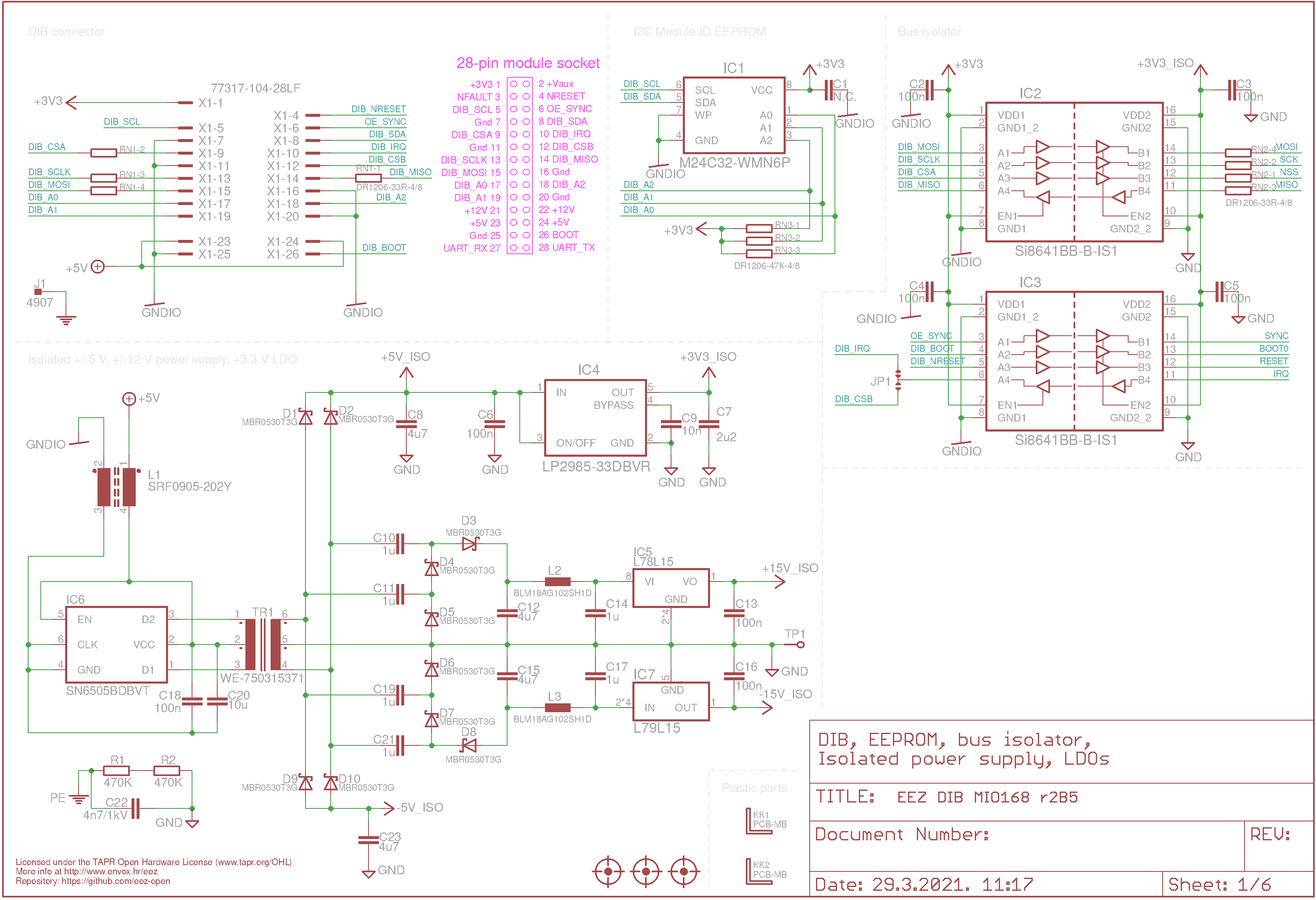
The MIO168 module interface with the MCU module is accomplished over the 28-pin 0.1” right angled header (X1). In order for all its inputs and outputs on the terminal to be “floated” with respect to the GND MCU modules, all signal lines as well as the power supply coming from the BP3C backplane must be isolated. This was achieved by using two digital isolators (IC2, IC3) for the signal lines.
To isolate +5 V used for powering the module, an isolated low-noise push-pull converter (IC6, TR1) is used, which gives ±5 V at the output, and the output from the quadrupler (D3-D8, C10-C12, C15, C19, C21) is additionally regulated with two LDOs (IC5, IC7) to obtain ±15 V. An additional LDO (IC1) is used to power the MCU operating at +3.3 V.
On-board I2C EEPROM (IC1) provides storage for module-specific information such as its ID, analog inputs and outputs calibration data and working hours counters. Its address is defined by RN3-1 to RN2-3 pull-up resistors and ground connections on the backplane.
STM32 Cortex M4 MCU
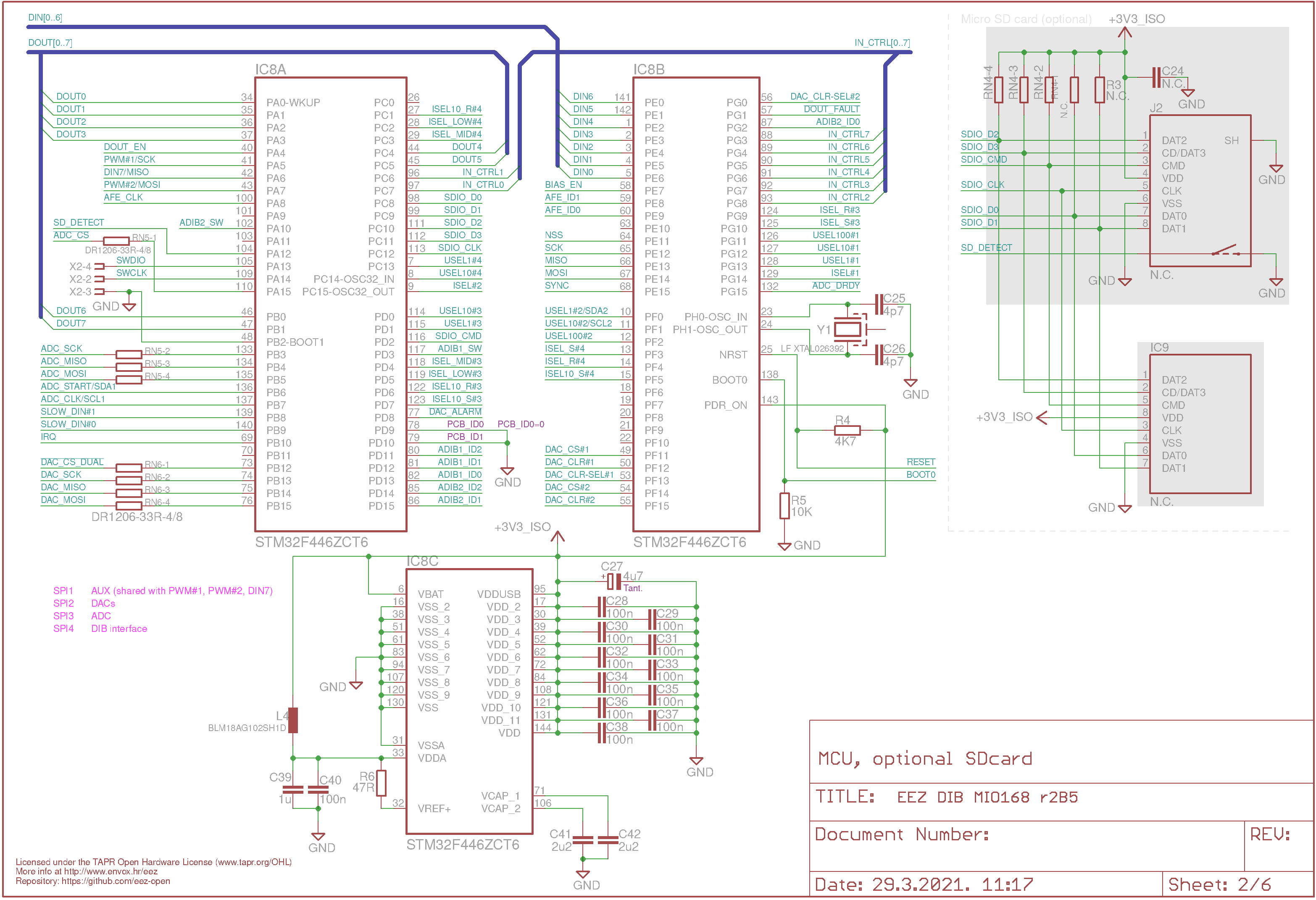
High-performance foundation line ARM Cortex-M4 MCU with DSP and FPU, 256 KiB Flash in LQFP-144 package is used to communicate with the master MCU on the MCU module and to control all resources including AFE expansion board when attached.
SPI is used to communicate with the master MCU and on-board peripherals. Programming its flash memory is also done via SPI, with BOOT0 and RST lines and can be easily accomplished via a touchscreen screen without the need for an external programmer/ debugger (ST-Link or similar).
Voltage/current mode DACs
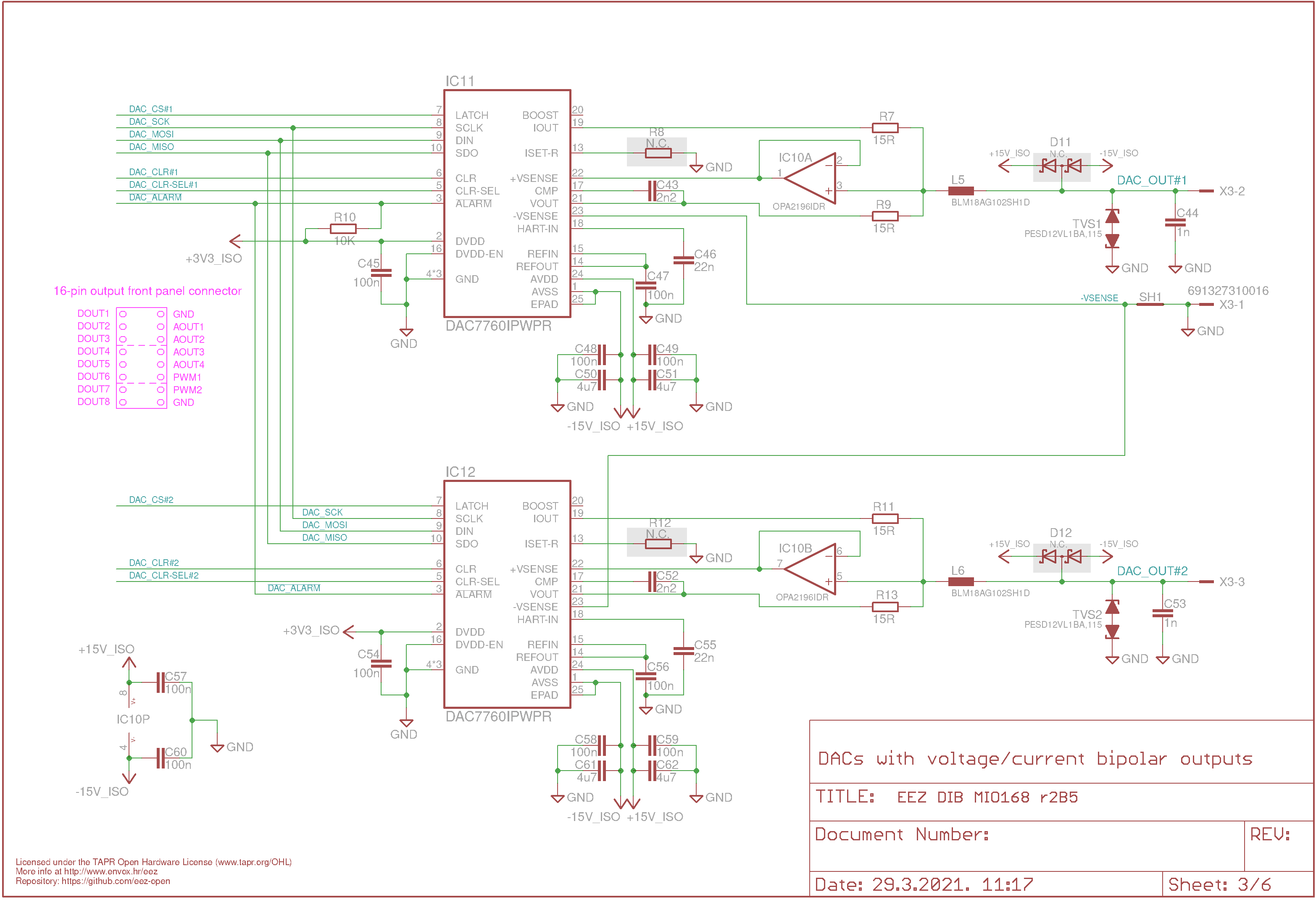
The first two outputs AOUT1 and AOUT2 (Fig. 4.) come from the DAC7660 (IC11, IC12), a 12-bit DAC that allows programmable setting of voltage or current mode in a total of 7 ranges (4 for voltage and 3 for current). When in voltage mode, the output can be unipolar or bipolar (up to ±10 V).
Both DACs have their own internal precision voltage reference of 5 V (10 PPM/°C).
Voltage mode DACS
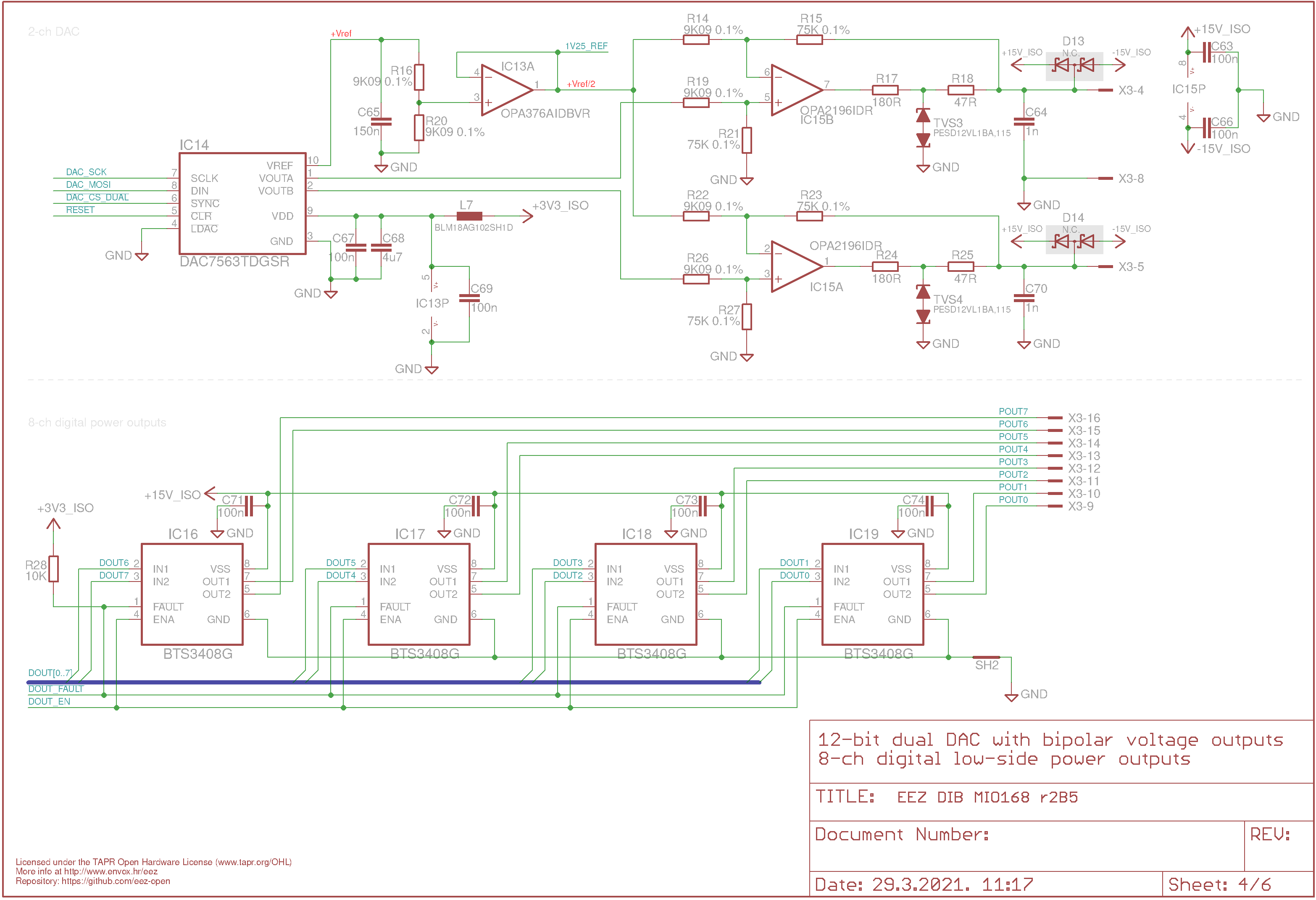
For the next two analog outputs AOUT3 and AOUT4 (Fig. 5.), a simpler, voltage-only dual channel DAC (IC14) mode with a unipolar signal is used. It also has its own precision voltage reference (+2.5 V, 4 PPM/°C). Its VREF output is used to obtain the +Vref/2 (R16/R20 voltage divider with IC13 buffer) required to set the reference point of the operational amplifiers (IC15A, IC15B) which are used to generate bipolar outputs in the ±10 V range (calibrated). All three DACs share the same SPI bus (SPI2).
Digital outputs
Eight digital outputs are obtained from four smart low-side power switches (IC16-IC19) with logic level inputs. They have multiple protections (overload, short circuit, over voltage, current limitation, thermal shutdown with out restart) and support switching frequencies up to 50 kHz.
Since these are low-side switches and not push-pull outputs, in order to see their activity it will be necessary to put some load or pull-up towards the external power supply which must not exceed 60 V.
Max. load per channel is 550 mA. The turn-on resistance of the switches is relatively low: 550 mΩ.
Digital inputs
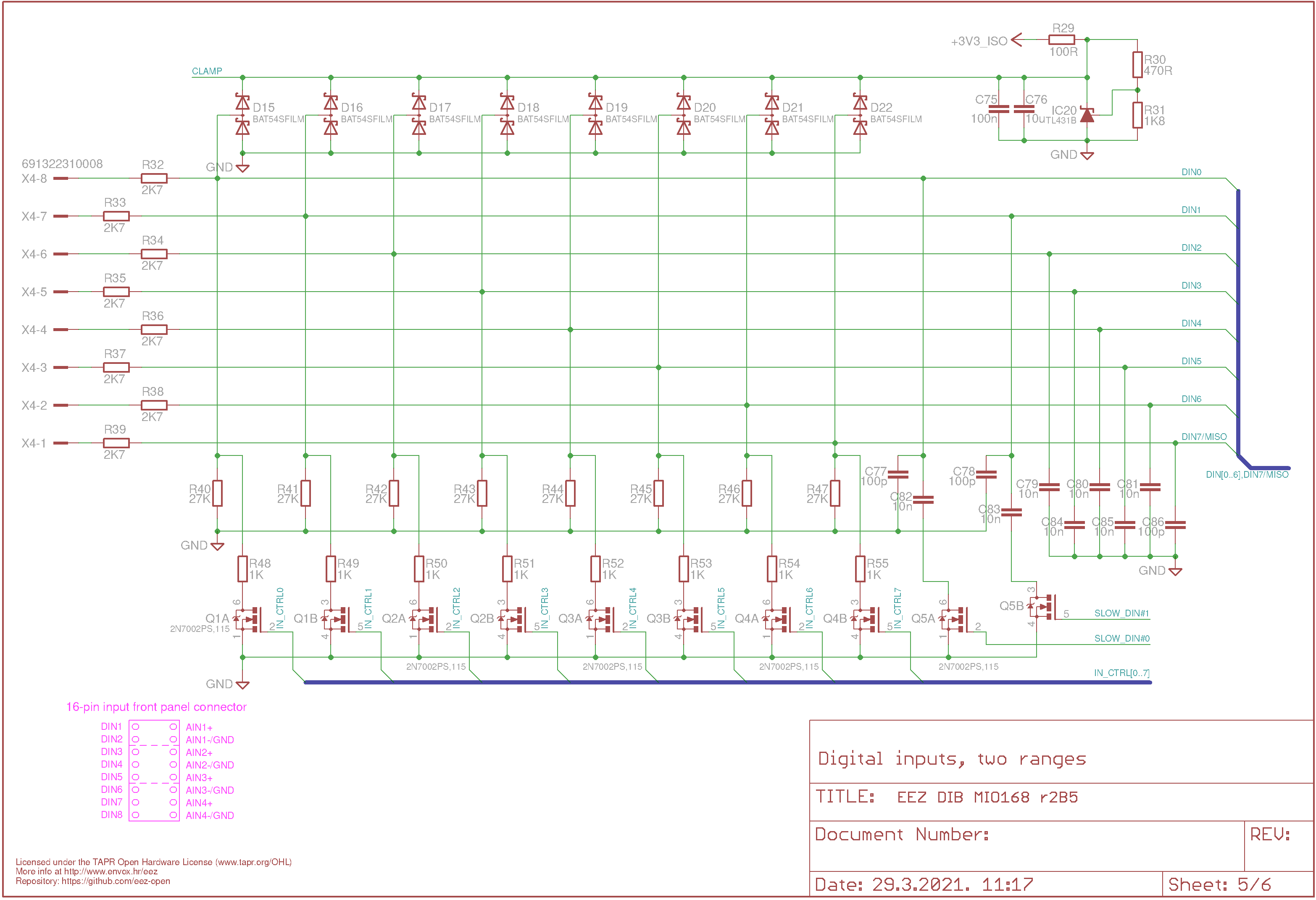
No special IC is used for the digital inputs, but eight inputs on the MCU are used. At the inputs there is level shifting for two ranges (+3.3/5 V and +12/24 V) and protection (D15-D22) with an active clamp on the positive power rail (IC20).
The input range selection can be defined for each channel individually using eight MOSFETs (dual in package, Q1-Q4) that switch the attenuation of the input voltage divider.
Two additional MOSFET switches (Q5) are used to lower the speed of the first two channels by adding capacitors C82, C83.
ADIB
The MIO168 module can be connected to other modules with two analog bidirectional lines. It uses two ADIB 10-pin connectors for this which have a signal pair surrounded by GND signals to reduce interference. Furthermore, three identification pins (ID0-ID2) are available to detect to which module the ADIB cable is connected.
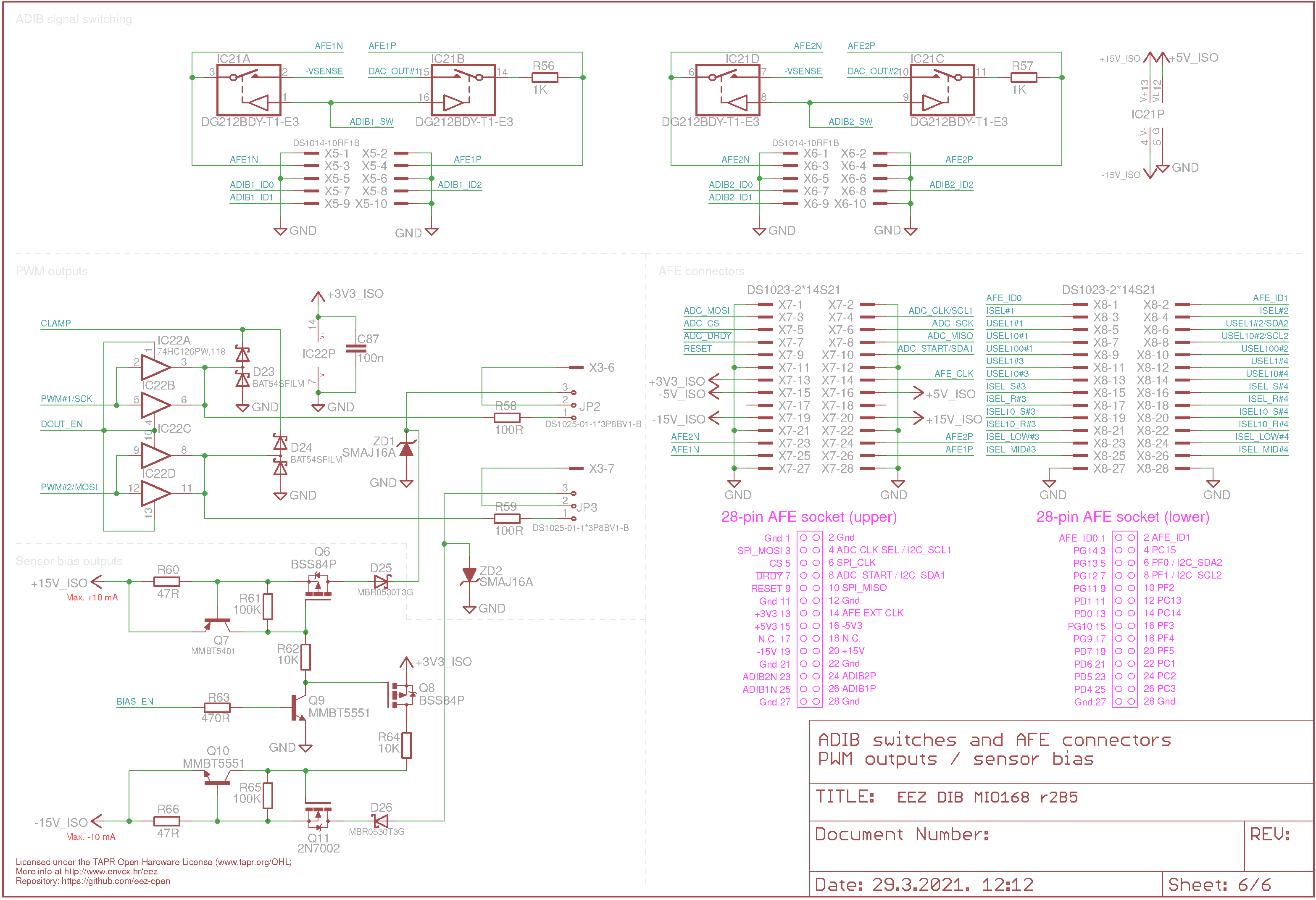
The MIO168 module can also redirect the first two analog outputs (AOUT1, AOUT2) via ADIB to other modules. Analog switches IC21A-IC21D are used for this. R56, R57 are in this case used to further limit the output current from the analog outputs.
Auxiliary power for sensors / PWM outputs
Pins X3-6 and X3-7 share two circuits: a symmetrical power supply and two square wave outputs and jumpers JP2 and JP3 are used for selection.
The symmetrical power supply is controlled by the BIAS_EN signal and can be used to power the sensors connected to the MIO168 inputs. The current is limited to ~10 mA so as not to overload the isolated DC-DC converter (IC6). The outputs are protected with ZD1/D25, and ZD2/D26.
Square wave outputs are connected to MCU PWM outputs, separated (IC22) and clamped (D34, D24). The same active clamp on the positive power rail was used as for the digital input (IC20).
AFE (Analog Front End) connectivity
The connection of the AFE extension board is provided with two 28-pin connectors (X7, X8). Three active-low pins (AFE_ID0 to AFE_ID2) are used for connected AFE identification.
All five power supplies are also available to the AFE extension board. The remaining pins are used for analog signals going to ADIB (AFE1P, AFE1N and AFE2P, AFE2N), for SPI communication and for managing AFE resources (control of voltage and current range selection, etc.).

