|
Current version |
r1B6 |
|
Status |
Completed, ready for production |
|
PCB manufactured |
Yes (r1B5) |
|
PCB assembled |
Yes (r1B5) |
|
BOM |
Yes (TME, Mouser, Digikey, Farnell, RS) |
|
File repository |
https://github.com/eez-open/dib-smx46 (include Eagle, Gerber and BOM files) |
|
License |
|
|
Contributions |
Feature list
- On-board STM32F030C6T6 ARM Cortex-M0 Value line MCU, 32 KiB Flash, 48 MHz CPU, LQFP-48 package
- 2 x 16-pin dual row 3.81 mm connectors
- 2 x ADIB connectors (10-pin 2 mm)
- 4 x 6 switch matrix (24 two-wire crosspoints), max. 2 A
- 1 x power relay, max. 8 A / 230 Vac
- 2 x analog output 0 – 10 V, 10 mV set resolution (12-bit)
- On-board +3.3 V LDO
- Firmware download via UART
- Optional SWD for debugging
- I2C EEPROM for storing board specific parameters
- Dimensions: 146 x 95 mm, 2-layer PCB
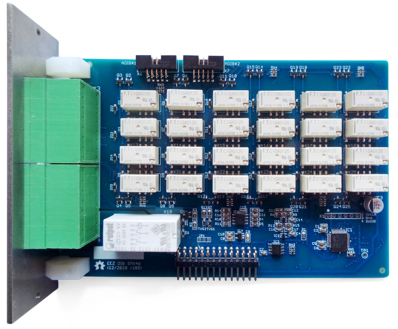
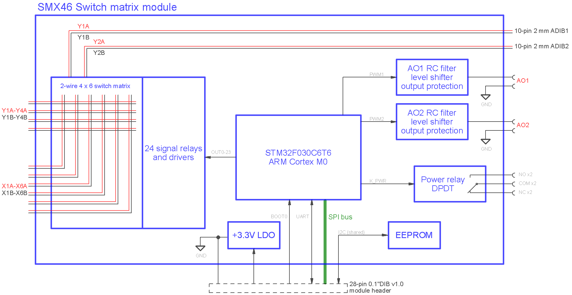
The SMX46 module offers a switch matrix of 24 signal 2-wire crosspoints organized into 4 rows and 6 columns. Additional functionalities are two analog outputs and one power relay with two SPDT (form C) switches.
The module has two 16-pin 3.81 mm connectors on the front panel thanks to which it is possible to quickly and easily connect the wires without the need for an additional breakout box. 8-way pluggable female terminal connector blocks in low-profile push-in and screw-fasten variants can be used to connect the wires.
EEZ DIB interface
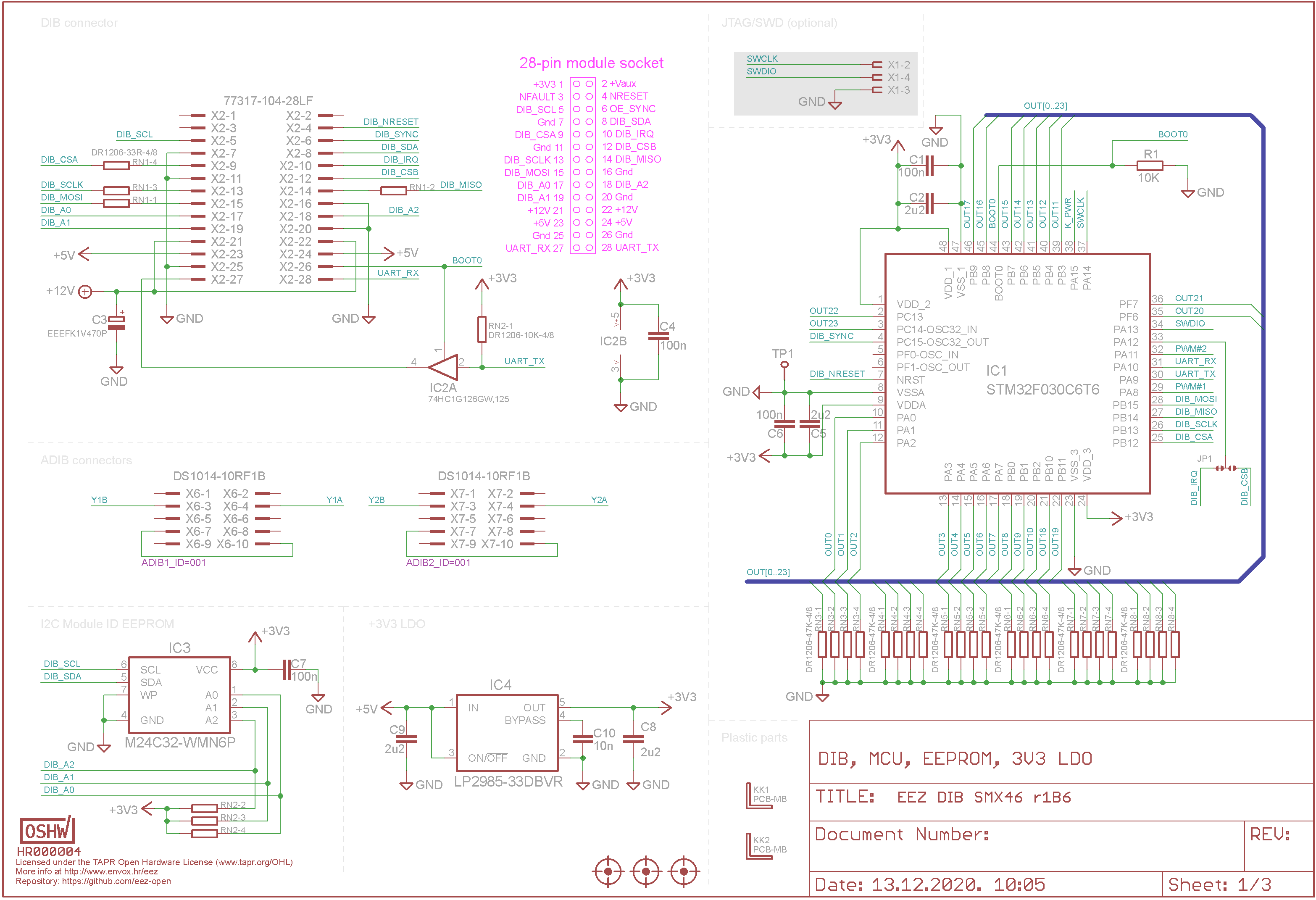
The SMX46 module interface with the MCU module is accomplished over the 28-pin 0.1” right angled header (X2).
On-board I2C EEPROM (IC3) provides storage for module-specific information such as its ID, analog outputs calibration data, working hours counters and relay switch cycles. Its address is defined by RN2-2 to RN2-4 pull-up resistors and ground connections on the backplane.
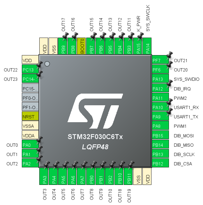
The STM32F030C6T6, a mainstream ARM Cortex-M0 Value line MCU with 32 KiB Flash, 48 MHz (IC1) is used to control power relays and to communicate with the master MCU on the MCU module.
UART and BOOT0 are used to program its flash memory, a process that is controlled by the master MCU and can be easily done via a touchscreen screen without the need for an external programmer/ debugger (ST-Link or similar). 3-state buffer (IC2) is used to control the UART TX output which can only be active while downloading the firmware to flash memory.
The powering of the MCU and all logic is done via 3.3 V LDO (IC4) which uses +5 V from DIB.
Two 10-pin 2.0 mm ADIB connectors (X6, X7) are used for internal connectivity with other modules (e.g. MIO168): Y1A/Y1B lines are exposed to ADIB #1 and Y2A/Y2B to ADIB #2. SMX46 ADIB ID is set to 001.
Switch matrix and power relay
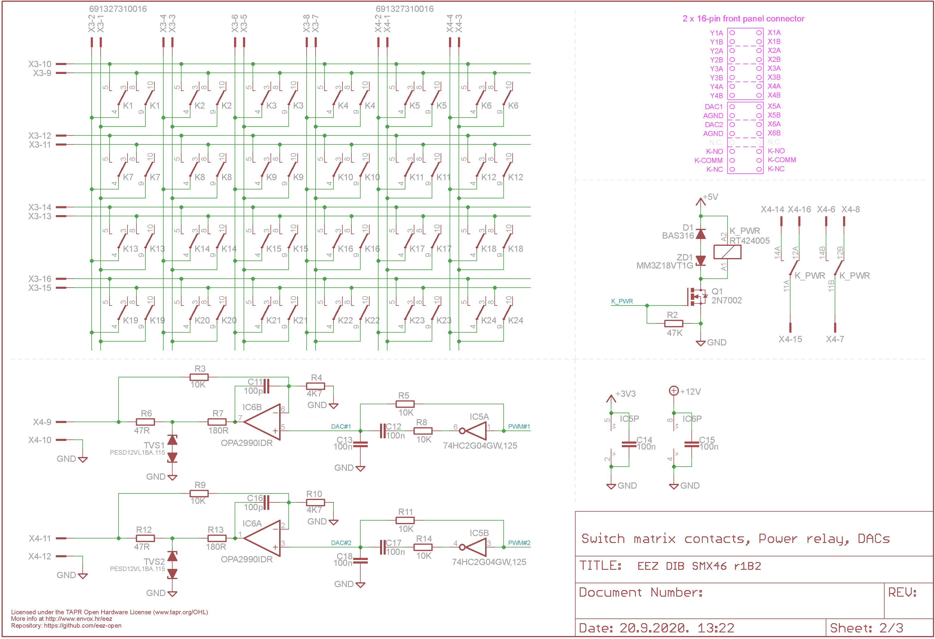
Two wire crosspoints switch matrix were made by contacting the signal relays K1 to K24 as shown in Fig. 5.
Matrix line pairs are exposed on the front panel connectors X3 and X4 and are denoted by the suffixes A and B: the columns have designations from X1A/X1B to X6A/X6B, and the rows Y1A/Y1B to Y4A/Y4B.
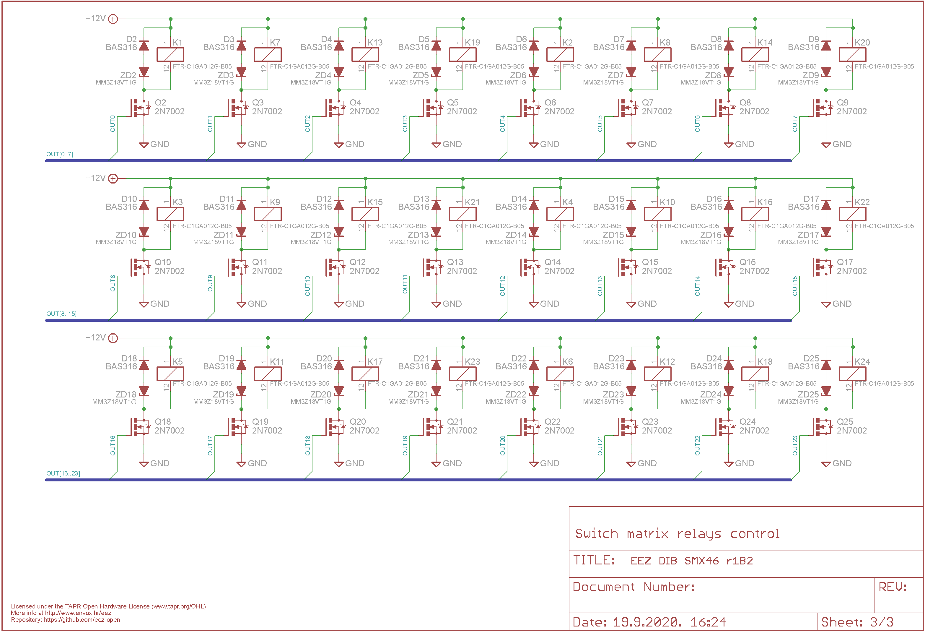
Low power MOSFETs (Q2 to Q25) are used to drive the switch matrix relays, whose inputs also have pull-down resistors (RN2-RN8, Fig. 4) for better immunity.
Relay coil suppression is accomplished by a combination of rectifier (D2 to D25) and zener (ZD2 to ZD25) diodes. This affords the best compromise both to coil switch protection (MOSFET) and relay switching performance and reliability. The relays are powered by +12 V which is filtered with C3.
The on-board power module (K1) offers switching of two additional circuits.
Analog outputs
The MCU used does not offer DAC outputs so PWM is used to generate analog signals. Conversion of PWM to analog signals is accomplished with DC filtering and additional ripple cancellation (IC5) as proposed by Stephen Woodward (see EDN article Cancel PWM DAC ripple with analog subtraction, November 28, 2017).
Since the PWM amplitude is +3.3 V, the generated analog signal cannot exceed this voltage. For this reason, a non-inverted op-amp (IC6) with a gain of about 3.13 is used so that the max non calibrated output voltage is just over 10 V (10.3 V).
The output current is limited by using R6 + R7 and R12 + R13, and TVS1 and TVS2 are used for overvoltage protection.

